8051 Architectural Specification and Functional Description
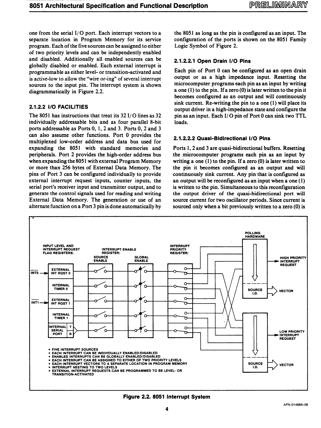
one from the serial I/O port. Each interrupt vectors to a separate location in Program Memory for its service program. Each ofthe five sources can be assigned to either of two priority levels and can be independently enabled and disabled. Additionally all enabled sources can be globally disabled or enabled. Each external interrupt is programmable as either level- or
2.1.2.21/0 FACILITIES
The 8051 has instructions that treat its 32 I/O lines as 32 individually addressable bits and as four parallel
the 8051 as long as the pin is configured as an input. The configuration of the ports is shown on the 8051 Family Logic Symbol of Figure 2.
2.1.2.2.1 Open Drain 1/0 Pins
Each pin of Port 0 can be configured as an open drain output or as a high impedance input. Resetting the microcomputer programs each pin as an input by writing
aone (I) to the pin. Ifa zero (0) is later written to the pin it becomes configured as an output and will continuously sink current.
2.1.2.2.2
Ports 1,2 and 3 are
|
|
|
|
| POLLING |
|
|
|
|
|
| HARDWARE |
|
| INPUT LEVEL AND |
|
| INTERRUPT |
| |
| INTERRUPT REQUEST | INTERRUPT ENABLE | PRIORITY |
| ||
| FLAG REGISTERS: | REGISTER: |
| REGISTER: |
| |
|
|
| SOURCE | GLOBAL |
| HIGH PRIORITY |
|
|
| ENABLE | ENABLE |
| INTERRUPT |
INTO | ...... | eXTERNAL |
| ..AI'" |
|
|
INTRQST0 |
|
| V |
| ||
|
|
|
|
| ||
|
|
|
| ...AI"'" |
| |
|
| INTERNAL | ..... | 1 | =>VECTOR | |
|
| TIMER 0 |
|
| SOURCE | |
tNT1 | ...... | EXTERNAL | - | I"'" | I.D. | |
INT RQST 1 |
|
|
| |||
|
|
|
|
|
| |
|
| INTERNAL |
| I'" |
|
|
|
| TIMER 1 |
|
|
|
|
INTERNAL~ | ,.. | r:. | - |
SERIAL | |||
PORT R |
|
|
•FIVE INTERRUPT SOURCES
•EACH INTERRUPT CAN BE INDIVIDUALLY ENABLED/DISABLED
•ENABLED INTERRUPTS CAN BE GLOBALLY ENABLED/DISABLED
•EACH INTERRUPT CAN BE ASSIGNED TO EITHER OF TWO PRIORITY LEVELS
•EACH INTERRUPT VECTORS TO A SEPARATE LOCATION IN PROGRAM MEMORY
•INTERRUPT NESTING TO TWO LEVELS
•EXTERNAL INTERRUPT REQUESTS CAN BE PROGRAMMED TO BE LEVEL- OR
| |
V |
|
~ | |
SOURCE | |
I.D. |
LOW PRIORITY INTERRUPT REQUEST
VECTOR
Figure 2.2. 8051 Interrupt System
4