8051 Architectural Specification and Functional Description
last data bit (i.e. ninth or tenth received bit) is sampled. As long as RI is set, the loading of SBUF, the updating of RB8 and the generation of further receiver interrupts is inhibited. Thus, overrun will occur if the programmer does not reset RI before reception of the next frame's last data bit since the receiver's input shift register will shift in a third frame.
The
+5V
2.13 EXTERNAL INTERFACE
2.13.1 Processor Reset and Initialization
Processor initialization is accomplished with activation of the RST /VPO pin. To reset the processor, this pin should be held high for at least
Register | Content |
PC | OOOOH |
SP | 07H |
PSW, OPH, OPL, A, B, | OOH |
IP, IE, SCaN, TCON, | OOH |
TMOO, THl, THO, | OOH |
TLl, TLO | OOH |
SBUF | Indeterminate |
Port | FFH (configures all I/O |
| pins as inputs) |
Internal RAM | Unchanged if VPO |
| applied; else |
| indeterminate |
Figure 2.53 Register Initialization
In addition, certain of the control pins are driven to a TTL high level during initialization. These are ALE/ PROG and PSEN. Thus, no ALE or PSEN signals are generated while RST / VPD is high. When the processor is reset all ports are immediately written with ones (l's).
+5V
t 8051
RSTNPD
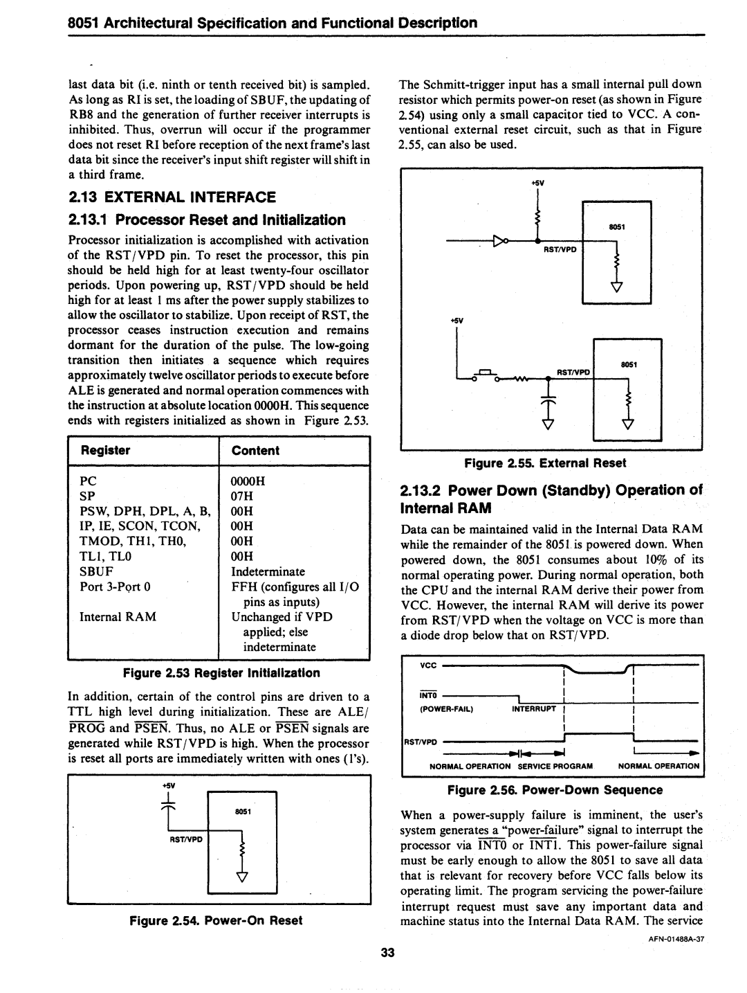
Figure 2.54. Power-On Reset
.... | 8051 |
| |
v | RSTNPD |
|
+5VL 8051
t
Figure 2.55. External Reset
2.13.2Power Down (Standby) Operation of Internal RAM
Data can be maintained valid in the Internal Data RAM while the remainder of the 8051 is powered down. When powered down, the 8051 consumes about 10% of its normal operating power. During normal operation, both the CPU and the internal RAM derive their power from VCC. However, the internal RAM will derive its power from RST/VPD when the voltage on VCC is more than a diode drop below that on RST/VPD.
VCC --------- i'......- ___rffl----
| I | I | |
| |||
(POWER·FAIL) | INTERRUPT I | I | |
|
| I | I |
|
| tl______ | |
|
| I | I |
RSTNPO | _ . | • | |
NORMAL OPERATION | SERVICE PROGRAM | NORMAL OPERATION | |
Figure 2.56. Power-Down Sequence
When a
33