8051 Architectural Specification and Functional Description
processing is especially effective in systems where controls in a complex process are required at physically separated locations.
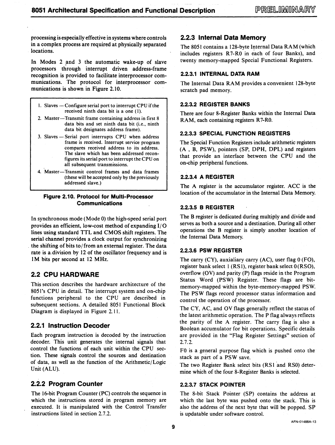
In Modes 2 and 3 the automatic
1.Slaves
2.
3.Slaves - Serial port interrupts CPU when address frame is received. Interrupt service program compares received address to its address. The slave which has been addressed recon- figures its serial port to interrupt the CPU on all subsequent transmissions.
4.
Figure 2.10. Protocol for Multi-Processor Communications
In synchronous mode (Mode 0) the
. the shifting of bits to/from an external register. The data rate is a.division by 12 of the oscillator frequency and is I M bits p(:r second at 12 MHz.
2.2 CPU HARDWARE
This section describes the hardware architecture of the 8051's CPU in detaiL The interrupt system and
2.2.1 Instruction Decoder
Each program instruction is decoded by the instruction decoder. This unit generates the internal signals that control the functions of each unit within the CPU sec- tion. These signals control the sources and destination of data, as well as the function of the Arithmetic/Logic Unit (ALU).
2.2.2 Program Counter
The
2.2.3 Internal Data Memory
The 8051 contains a
2.2.3.1 INTERNAL DATA RAM
The Internal Data RAM provides a convenient
2.2.3.2 REGISTER BANKS
There are four
2.2.3.3 SPECIAL FUNCTION REGISTERS
The Special Function Registers include arithmetic registers (A , B, PSW), pointers (SP, DPH, DPL) and registers that provide an interface between the CPU and the
2.2.3.4 A REGISTER
The A register is the accumulator register. ACC is the location of the accumulator in the Internal Data Memory.
2.2.3.5 B REGISTER
The B register is dedicated during multiply and divide and serves as both a source and a destination. During all other operations the B register is simply another location of the Internal Data Memory.
2.2.3.6 PSW REGISTER
The carry (CY), auxialiary carry (AC), user flag 0 (FO), register bank select I (RS I), register bank select 0 (RSO), overflow (OV) and parity (P) flags reside in the Program Status Word (PSW) Register. These flags are bit-
The CY, AC, and OV flags generally reflect the status of the latest arithmetic operation. The P flag always reflects the parity of the A register. The carry flag is also a Boolean accumulator for bit operations. Specific details are provided in the "Flag Register Settings" section of 2.7.2.
FO is a general purpose flag which is pushed onto the stack as part of a PSW save.
The two Register Bank select bits (RS I 'and RSO) deter- mine which of the four
2.2.3.7 STACK POINTER
The
9