7521Plus / N N/B MAINTENANCE
5. Pin Descriptions Of Major Components
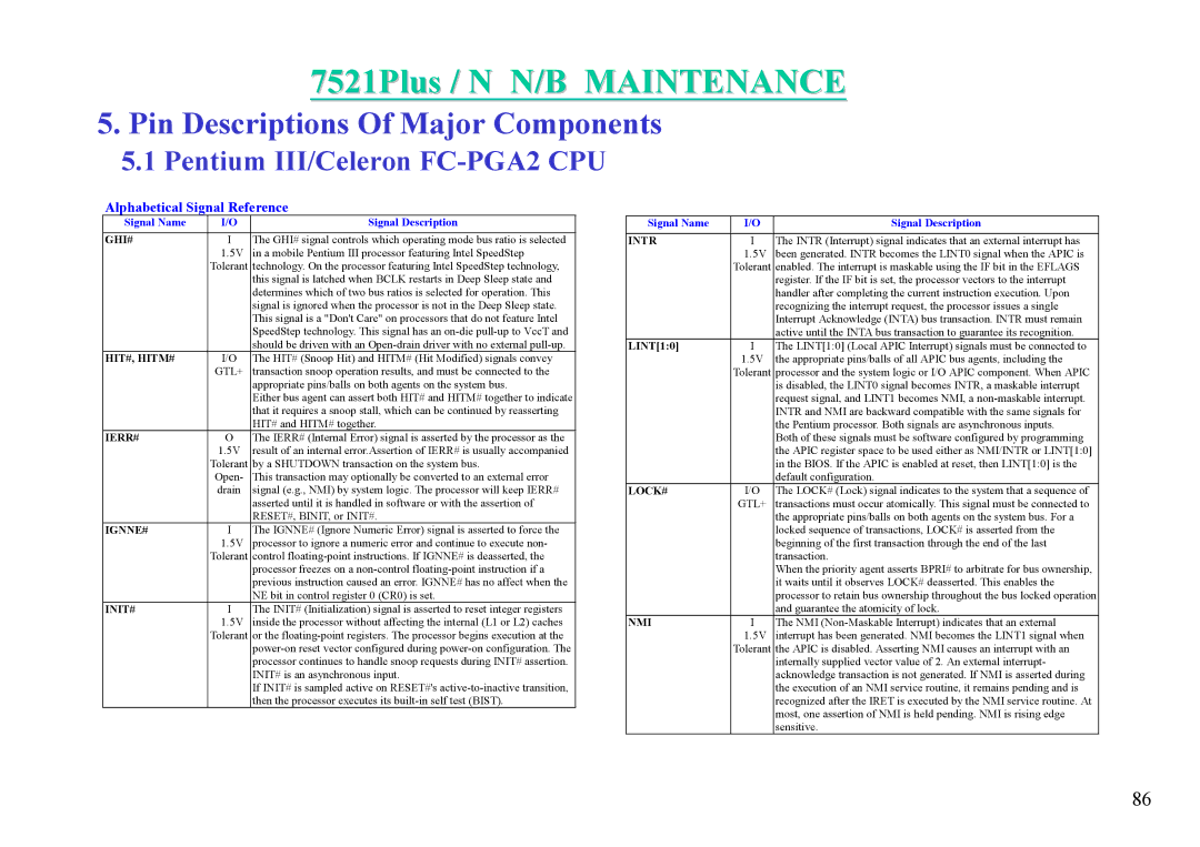
5.1 Pentium III/Celeron FC-PGA2 CPU
Alphabetical Signal Reference
Signal Name | I/O | Signal Description |
GHI# | I | The GHI# signal controls which operating mode bus ratio is selected |
| 1.5V | in a mobile Pentium III processor featuring Intel SpeedStep |
| Tolerant | technology. On the processor featuring Intel SpeedStep technology, |
|
| this signal is latched when BCLK restarts in Deep Sleep state and |
|
| determines which of two bus ratios is selected for operation. This |
|
| signal is ignored when the processor is not in the Deep Sleep state. |
|
| This signal is a "Don't Care" on processors that do not feature Intel |
|
| SpeedStep technology. This signal has an |
|
| should be driven with an |
HIT#, HITM# | I/O | The HIT# (Snoop Hit) and HITM# (Hit Modified) signals convey |
| GTL+ | transaction snoop operation results, and must be connected to the |
|
| appropriate pins/balls on both agents on the system bus. |
|
| Either bus agent can assert both HIT# and HITM# together to indicate |
|
| that it requires a snoop stall, which can be continued by reasserting |
|
| HIT# and HITM# together. |
IERR# | O | The IERR# (Internal Error) signal is asserted by the processor as the |
| 1.5V | result of an internal error.Assertion of IERR# is usually accompanied |
| Tolerant | by a SHUTDOWN transaction on the system bus. |
| Open- | This transaction may optionally be converted to an external error |
| drain | signal (e.g., NMI) by system logic. The processor will keep IERR# |
|
| asserted until it is handled in software or with the assertion of |
|
| RESET#, BINIT, or INIT#. |
IGNNE# | I | The IGNNE# (Ignore Numeric Error) signal is asserted to force the |
| 1.5V | processor to ignore a numeric error and continue to execute non- |
| Tolerant | control |
|
| processor freezes on a |
|
| previous instruction caused an error. IGNNE# has no affect when the |
|
| NE bit in control register 0 (CR0) is set. |
INIT# | I | The INIT# (Initialization) signal is asserted to reset integer registers |
| 1.5V | inside the processor without affecting the internal (L1 or L2) caches |
| Tolerant | or the |
|
| |
|
| processor continues to handle snoop requests during INIT# assertion. |
|
| INIT# is an asynchronous input. |
|
| If INIT# is sampled active on RESET#'s |
|
| then the processor executes its |
Signal Name | I/O | Signal Description |
INTR | I | The INTR (Interrupt) signal indicates that an external interrupt has |
| 1.5V | been generated. INTR becomes the LINT0 signal when the APIC is |
| Tolerant | enabled. The interrupt is maskable using the IF bit in the EFLAGS |
|
| register. If the IF bit is set, the processor vectors to the interrupt |
|
| handler after completing the current instruction execution. Upon |
|
| recognizing the interrupt request, the processor issues a single |
|
| Interrupt Acknowledge (INTA) bus transaction. INTR must remain |
|
| active until the INTA bus transaction to guarantee its recognition. |
LINT[1:0] | I | The LINT[1:0] (Local APIC Interrupt) signals must be connected to |
| 1.5V | the appropriate pins/balls of all APIC bus agents, including the |
| Tolerant | processor and the system logic or I/O APIC component. When APIC |
|
| is disabled, the LINT0 signal becomes INTR, a maskable interrupt |
|
| request signal, and LINT1 becomes NMI, a |
|
| INTR and NMI are backward compatible with the same signals for |
|
| the Pentium processor. Both signals are asynchronous inputs. |
|
| Both of these signals must be software configured by programming |
|
| the APIC register space to be used either as NMI/INTR or LINT[1:0] |
|
| in the BIOS. If the APIC is enabled at reset, then LINT[1:0] is the |
|
| default configuration. |
LOCK# | I/O | The LOCK# (Lock) signal indicates to the system that a sequence of |
| GTL+ | transactions must occur atomically. This signal must be connected to |
|
| the appropriate pins/balls on both agents on the system bus. For a |
|
| locked sequence of transactions, LOCK# is asserted from the |
|
| beginning of the first transaction through the end of the last |
|
| transaction. |
|
| When the priority agent asserts BPRI# to arbitrate for bus ownership, |
|
| it waits until it observes LOCK# deasserted. This enables the |
|
| processor to retain bus ownership throughout the bus locked operation |
|
| and guarantee the atomicity of lock. |
NMI | I | The NMI |
| 1.5V | interrupt has been generated. NMI becomes the LINT1 signal when |
| Tolerant | the APIC is disabled. Asserting NMI causes an interrupt with an |
|
| internally supplied vector value of 2. An external interrupt- |
|
| acknowledge transaction is not generated. If NMI is asserted during |
|
| the execution of an NMI service routine, it remains pending and is |
|
| recognized after the IRET is executed by the NMI service routine. At |
|
| most, one assertion of NMI is held pending. NMI is rising edge |
|
| sensitive. |
86