7521Plus / N N/B MAINTENANCE
5. Pin Descriptions Of Major Components
5.1 Pentium III/Celeron FC-PGA2 CPU
Alphabetical Signal Reference
Signal Name | I/O | Signal Description |
PICCLK | I | The PICCLK (APIC Clock) signal is an input clock to the processor |
| 2.5V | and system logic or I/O APIC that is required for operation of the |
| Tolerant | processor, system logic, and I/O APIC components on the APIC bus. |
PICD[1:0] | I/O | The PICD[1:0] (APIC Data) signals are used for |
| 1.5V | message passing on the APIC bus. They must be connected to the |
| Tolerant | appropriate pins/balls of all APIC bus agents, including the processor |
| Open- | and the system logic or I/O APIC components. If the PICD0 signal is |
| drain | sampled low on the |
|
| signal, then the APIC is hardware disabled. |
PLL1, PLL2 | Analog | The PLL1 and PLL2 signals provide isolated analog decoupling is |
|
| required for the internal PLL. See Section 3.2.2 for a description of |
|
| the analog decoupling circuit. |
PRDY# | O | The PRDY# (Probe Ready) signal is a processor output used by |
| GTL+ | debug tools to determine processor debug readiness. |
PREQ# | I | The PREQ# (Probe Request) signal is used by debug tools to request |
| 1.5V | debug operation of the processor. |
| Tolerant |
|
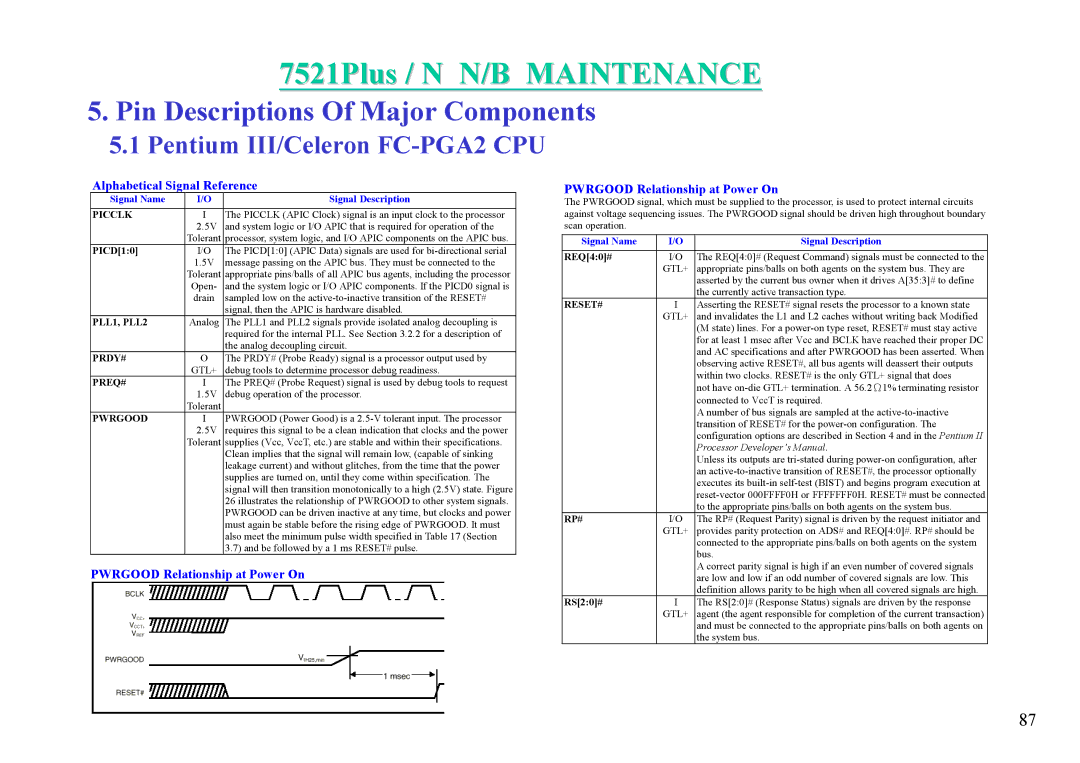
PWRGOOD | I | PWRGOOD (Power Good) is a |
| 2.5V | requires this signal to be a clean indication that clocks and the power |
| Tolerant | supplies (Vcc, VccT, etc.) are stable and within their specifications. |
|
| Clean implies that the signal will remain low, (capable of sinking |
|
| leakage current) and without glitches, from the time that the power |
|
| supplies are turned on, until they come within specification. The |
|
| signal will then transition monotonically to a high (2.5V) state. Figure |
|
| 26 illustrates the relationship of PWRGOOD to other system signals. |
|
| PWRGOOD can be driven inactive at any time, but clocks and power |
|
| must again be stable before the rising edge of PWRGOOD. It must |
|
| also meet the minimum pulse width specified in Table 17 (Section |
|
| 3.7) and be followed by a 1 ms RESET# pulse. |
PWRGOOD Relationship at Power On
PWRGOOD Relationship at Power On
The PWRGOOD signal, which must be supplied to the processor, is used to protect internal circuits against voltage sequencing issues. The PWRGOOD signal should be driven high throughout boundary scan operation.
Signal Name | I/O | Signal Description |
REQ[4:0]# | I/O | The REQ[4:0]# (Request Command) signals must be connected to the |
| GTL+ | appropriate pins/balls on both agents on the system bus. They are |
|
| asserted by the current bus owner when it drives A[35:3]# to define |
|
| the currently active transaction type. |
RESET# | I | Asserting the RESET# signal resets the processor to a known state |
| GTL+ | and invalidates the L1 and L2 caches without writing back Modified |
|
| (M state) lines. For a |
|
| for at least 1 msec after Vcc and BCLK have reached their proper DC |
|
| and AC specifications and after PWRGOOD has been asserted. When |
|
| observing active RESET#, all bus agents will deassert their outputs |
|
| within two clocks. RESET# is the only GTL+ signal that does |
|
| not have |
|
| connected to VccT is required. |
|
| A number of bus signals are sampled at the |
|
| transition of RESET# for the |
|
| configuration options are described in Section 4 and in the Pentium II |
|
| Processor Developer’s Manual. |
|
| Unless its outputs are |
|
| an |
|
| executes its |
|
| |
|
| to the appropriate pins/balls on both agents on the system bus. |
RP# | I/O | The RP# (Request Parity) signal is driven by the request initiator and |
| GTL+ | provides parity protection on ADS# and REQ[4:0]#. RP# should be |
|
| connected to the appropriate pins/balls on both agents on the system |
|
| bus. |
|
| A correct parity signal is high if an even number of covered signals |
|
| are low and low if an odd number of covered signals are low. This |
|
| definition allows parity to be high when all covered signals are high. |
RS[2:0]# | I | The RS[2:0]# (Response Status) signals are driven by the response |
| GTL+ | agent (the agent responsible for completion of the current transaction) |
|
| and must be connected to the appropriate pins/balls on both agents on |
|
| the system bus. |
87