7521Plus / N N/B MAINTENANCE
5.Pin Descriptions Of Major Components
5.2SiS630S Slot 1/Socket 370 2D/3D Ultra-AGP™ Single Chipset
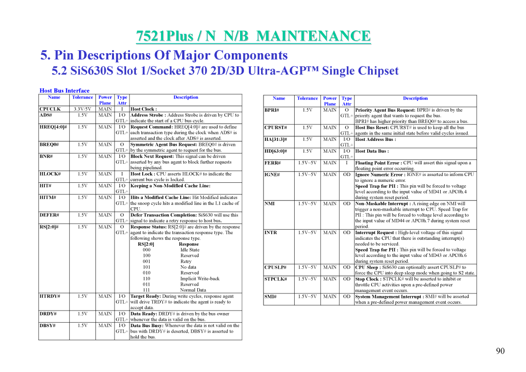
Host Bus Interface
Name | Tolerance | Power | Type |
| Description |
|
| Plane | Attr |
|
|
CPUCLK | 3.3V/5V | MAIN | I | Host Clock : |
|
ADS# | 1.5V | MAIN | I/O | Address Strobe : Address Strobe is driven by CPU to | |
|
|
| GTL+ | indicate the start of a CPU bus cycle. | |
HREQ[4:0]# | 1.5V | MAIN | I/O | Request Command: HREQ[4:0]# are used to define | |
|
|
| GTL+ | each transaction type during the clock when ADS# is | |
|
|
|
| asserted and the clock after ADS# is asserted. | |
BREQ0# | 1.5V | MAIN | O | Symmetric Agent Bus Request: BREQ0# is driven | |
|
|
| GTL+ | by the symmetric agent to request for the bus. | |
BNR# | 1.5V | MAIN | I/O | Block Next Request: This signal can be driven | |
|
|
| GTL+ | asserted by any bus agent to block further requests | |
|
|
|
| being pipelined. |
|
HLOCK# | 1.5V | MAIN | I | Host Lock : CPU asserts HLOCK# to indicate the | |
|
|
| GTL+ | current bus cycle is locked. | |
HIT# | 1.5V | MAIN | I/O | Keeping a | |
|
|
| GTL+ |
|
|
HITM# | 1.5V | MAIN | I/O | Hits a Modified Cache Line: Hit Modified indicates | |
|
|
| GTL+ | the snoop cycle hits a modified line in the L1 cache of | |
|
|
|
| CPU. |
|
DEFER# | 1.5V | MAIN | O | Defer Transaction Completion: SiS630 will use this | |
|
|
| GTL+ | signal to indicate a retry response to host bus. | |
RS[2:0]# | 1.5V | MAIN | O | Response Status: RS[2:0]# are driven by the response | |
|
|
| GTL+ | agent to indicate the transaction response type. The | |
|
|
|
| following shows the response type. | |
|
|
|
| RS[2:0] | Response |
|
|
|
| 000 | Idle State |
|
|
|
| 100 | Reserved |
|
|
|
| 001 | Retry |
|
|
|
| 101 | No data |
|
|
|
| 010 | Reserved |
|
|
|
| 110 | Implicit |
|
|
|
| 011 | Reserved |
|
|
|
| 111 | Normal Data |
HTRDY# | 1.5V | MAIN | I/O | Target Ready: During write cycles, response agent | |
|
|
| GTL+ | will drive TRDY# to indicate the agent is ready to | |
|
|
|
| accept data. |
|
DRDY# | 1.5V | MAIN | I/O | Data Ready: DRDY# is driven by the bus owner | |
|
|
| GTL+ | whenever the data is valid on the bus. | |
DBSY# | 1.5V | MAIN | I/O | Data Bus Busy: Whenever the data is not valid on the | |
|
|
| GTL+ | bus with DRDY# is deserted, DBSY# is asserted to | |
|
|
|
| hold the bus. |
|
Name | Tolerance | Power | Type |
| Description |
|
| Plane | Attr |
|
|
BPRI# | 1.5V | MAIN | O |
| Priority Agent Bus Request: BPRI# is driven by the |
|
|
| GTL+ | priority agent that wants to request the bus. | |
|
|
|
|
| BPRI# has higher priority than BREQ0# to access a bus. |
CPURST# | 1.5V | MAIN | O |
| Host Bus Reset: CPURST# is used to keep all the bus |
|
|
| GTL+ |
| agents in the same initial state before valid cycles issued. |
HA[31:3]# | 1.5V | MAIN | I/O |
| Host Address Bus : |
|
|
| GTL+ |
|
|
HD[63:0]# | 1.5V | MAIN | I/O |
| Host Data Bus : |
|
|
| GTL+ |
|
|
FERR# | 1.5V~5V | MAIN | I |
| Floating Point Error : CPU will assert this signal upon a |
|
|
|
|
| floating point error occurring. |
IGNE# | 1.5V~5V | MAIN | OD |
| Ignore Numeric Error : IGNE# is asserted to inform CPU |
|
|
|
|
| to ignore a numeric error. |
|
|
|
|
| Speed Trap for PII : This pin will be forced to voltage |
|
|
|
|
| level according to the input value of MD41 or APC0h.4 |
|
|
|
|
| during system reset period. |
NMI | 1.5V~5V | MAIN | OD |
|
|
|
|
|
|
| trigger a |
|
|
|
|
| PII : This pin will be forced to voltage level according to |
|
|
|
|
| the input value of MD44 or APC0h.7 during system reset |
|
|
|
|
| period. |
INTR | 1.5V~5V | MAIN | OD |
| Interrupt Request : |
|
|
|
|
| indicates the CPU that there is outstanding interrupt(s) |
|
|
|
|
| needed to be serviced. |
|
|
|
|
| Speed Trap for PII : This pin will be forced to voltage |
|
|
|
|
| level according to the input value of MD43 or APC0h.6 |
|
|
|
|
| during system reset period. |
CPUSLP# | 1.5V~5V | MAIN | OD |
| CPU Sleep : SiS630 can optionally assert CPUSLP# to |
|
|
|
|
| force the CPU into deep sleep mode when going to S2 state. |
STPCLK# | 1.5V~5V | MAIN | OD |
| Stop Clock : STPCLK# will be asserted to inhibit or |
|
|
|
|
| throttle CPU activities upon a |
|
|
|
|
| management event occurs. |
SMI# | 1.5V~5V | MAIN | OD |
| System Management Interrupt : SMI# will be asserted |
|
|
|
|
| when a |
90