7521Plus / N N/B MAINTENANCE
5. Pin Descriptions Of Major Components
5.1 Pentium III/Celeron FC-PGA2 CPU
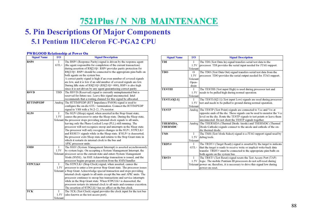
PWRGOOD Relationship at Power On
Signal Name | I/O | Signal Description |
RSP# | I | The RSP# (Response Parity) signal is driven by the response agent |
| GTL+ | (the agent responsible for completion of the current transaction) |
|
| during assertion of RS[2:0]#. RSP# provides parity protection for |
|
| RS[2:0]#. RSP# should be connected to the appropriate pins/balls on |
|
| both agents on the system bus. |
|
| A correct parity signal is high if an even number of covered signals |
|
| are low, and it is low if an odd number of covered signals are low. |
|
| During Idle state of RS[2:0]# (RS[2:0]#=000), RSP# is also high |
|
| since it is not driven by any agent guaranteeing correct parity. |
RSVD | TBD | The RSVD (Reserved) signal is currently unimplemented but is |
|
| reserved for future use. Leave this signal unconnected. Intel |
|
| recommends that a routing channel for this signal be allocated. |
RTTIMPEDP | Analog | The RTTIMPEDP (RTT Impedance/PMOS) signal is used to |
|
| configure the |
|
| signal to VSS with a |
SLP# | I | The SLP# (Sleep) signal, when asserted in the Stop Grant state, |
| 1.5V | causes the processor to enter the Sleep state. During the Sleep state, |
| Tolerant | the processor stops providing internal clock signals to all units, |
|
| leaving only the |
|
| processor will not recognize snoop and interrupts in the Sleep state. |
|
| The processor will only recognize changes in the SLP#, STPCLK# |
|
| and RESET# signals while in the Sleep state. If SLP# is deasserted, |
|
| the processor exits Sleep state and returns to the Stop Grant state in |
|
| which it restarts its internal clock to the bus and |
|
| APIC processor units. |
SMI# | I | The SMI# (System Management Interrupt) is asserted asynchronously |
| 1.5V | by system logic. On accepting a System Management Interrupt, the |
| Tolerant | processor saves the current state and enters System Management |
|
| Mode (SMM). An SMI Acknowledge transaction is issued, and the |
|
| processor begins program execution from the SMM handler. |
STPCLK# | I | The STPCLK# (Stop Clock) signal, when asserted, causes the |
| 1.5V | processor to enter a |
| Tolerant | a Stop Grant Acknowledge special transaction and stops providing |
|
| internal clock signals to all units except the bus and APIC units. The |
|
| processor continues to snoop bus transactions and service interrupts |
|
| while in the Stop Grant state. When STPCLK# is deasserted, the |
|
| processor restarts its internal clock to all units and resumes execution. |
|
| The assertion of STPCLK# has no affect on the bus clock. |
TCK | I | The TCK (Test Clock) signal provides the clock input for the test bus |
| 1.5V | (also known as the test access port). |
| Tolerant |
|
Signal Name | I/O | Signal Description |
TDI | I | The TDI (Test Data In) signal transfers serial test data to the |
| 1.5V | processor. TDI provides the serial input needed for JTAG support. |
| Tolerant |
|
TDO | O | The TDO (Test Data Out) signal transfers serial test data from the |
| 1.5V | processor. TDO provides the serial output needed for JTAG support. |
| Tolerant |
|
| Open- |
|
| drain |
|
TESTHI | I | The TESTHI (Test input High) is used during processor test and |
| 1.5V | needs to be pulled high during normal operation. |
| Tolerant |
|
TESTLO[2:1] | I | The TESTLO[2:1] (Test input Low) signals are used during processor |
| 1.5V | test and needs to be pulled to ground during normal operation. |
| Tolerant |
|
TESTP | Analog | The TESTP (Test Point) signals are connected to Vcc and Vss at |
|
| opposite ends of the die. These signals can be used to monitor the Vcc |
|
| level on the die. Route the TESTP signals to test points or leave them |
|
| unconnected. Do not short the TESTP signals together. |
THERMDA, | Analog | The THERMDA (Thermal Diode Anode) and THERMDC (Thermal |
THERMDC |
| Diode Cathode) signals connect to the anode and cathode of the on- |
|
| die thermal diode. |
TMS | I | The TMS (Test Mode Select) signal is a JTAG support signal used by |
| 1.5V | debug tools. |
| Tolerant |
|
TRDY# | I | The TRDY# (Target Ready) signal is asserted by the target to indicate |
| GTL+ | that the target is ready to receive write or implicit |
|
| transfer. TRDY# must be connected to the appropriate pins/balls on |
|
| both agents on the system bus. |
TRST# | I | The TRST# (Test Reset) signal resets the Test Access Port (TAP) |
| 1.5V | logic. The mobile Pentium III processors do not |
| Tolerant | power on; therefore, it is necessary to drive this signal low during |
|
|
88