7521Plus / N N/B MAINTENANCE
5.Pin Descriptions Of Major Components
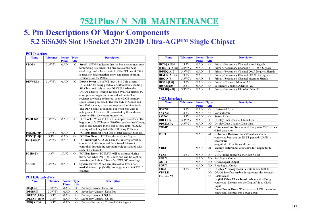
5.2SiS630S Slot 1/Socket 370 2D/3D Ultra-AGP™ Single Chipset
PCI Interface
Name | Tolerance | Power | Type | Description |
|
| Plane | Attr |
|
STOP# | 3.3V/5V | MAIN | I/O | Stop# : STOP# indicates that the bus master must start |
|
|
|
| terminating its current PCI bus cycle at the next |
|
|
|
| clock edge and release control of the PCI bus. STOP# |
|
|
|
| is used for disconnection, retry, and |
|
|
|
| sequences on the PCI bus. |
DEVSEL# | 3.3V/5V | MAIN | I/O | Device Select : As a PCI target, SiS Chip asserts |
|
|
|
| DEVSEL# by doing positive or subtractive decoding. |
|
|
|
| SiS Chip positively asserts DEVSEL# when the |
|
|
|
| DRAM address is being accessed by a PCI master, PCI |
|
|
|
| configuration registers or embedded controllers’ |
|
|
|
| registers are being addressed, or the BIOS memory |
|
|
|
| space is being accessed. The low 16K I/O space and |
|
|
|
| low 16M memory space are responded subtractively. |
|
|
|
| The DEVESEL# is an input pin when SiS Chip is |
|
|
|
| acting as a PCI master. It is asserted by the addressed |
|
|
|
| agent to claim the current transaction. |
PLOCK# | 3.3V/5V | MAIN | I/O | PCI Lock : When PLOCK# is sampled asserted at the |
|
|
|
| beginning of a PCI cycle, SiS630 considers itself being |
|
|
|
| locked and remains in the locked state until PLOCK# |
|
|
|
| is sampled and negated at the following PCI cycle. |
PREQ[2:0]# | 3.3V/5V | MAIN | I | PCI Bus Request : PCI Bus Master Request Signals |
PGNT[2:0]# | 3.3V | MAIN | O | PCI Bus Grant : PCI Bus Master Grant Signals |
INT[A:D]# | 3.3V/5V | MAIN | I | PCI interrupt A,B,C,D : The PCI interrupts will be |
|
|
|
| connected to the inputs of the internal Interrupt |
|
|
|
| controller through the rerouting logic associated with |
|
|
|
| each PCI interrupt. |
PCIRST# | 3.3V | AUX | O | PCI Bus Reset : PCIRST# will be asserted during |
|
|
|
| the period when PWROK is low, and will be kept on |
|
|
|
| asserting until about 24ms after PWROK goes high. |
SERR# | 3.3V/5V | MAIN | I | System Error : When sampled active low, a non- |
|
|
|
| maskable interrupt (NMI) can be generated to CPU if |
|
|
|
| enabled. |
PCI IDE Interface
Name | Tolerance | Power | Type | Description |
|
| Plane | Attr |
|
IDA[15:0] | 3.3V/5V | MAIN | I/O | Primary Channel Data Bus |
IDB[15:0] | 3.3V/5V | MAIN | I/O | Secondary Channel Data Bus |
IDECSA[1:0]# | 3.3V | MAIN | O | Primary Channel CS[1:0] |
IDECSB[1:0]# | 3.3V | MAIN | O | Secondary Channel CS[1:0] |
IIOR[A:B]# | 3.3V | MAIN | O | Primary/Secondary Channel IOR# Signals |
Name | Tolerance | Power | Type | Description |
|
| Plane | Attr |
|
IIOW[A:B]# | 3.3V | MAIN | O | Primary/Secondary Channel IOW# Signals |
ICHRDY[A:B] | 3.3V/5V | MAIN | I | Primary/Secondary Channel ICHRDY# Signals |
IDREQ[A:B] | 3.3V/5V | MAIN | I | Primary/Secondary Channel DMA Request Signals |
IDACK[A:B]# | 3.3V | MAIN | O | Primary/Secondary Channel DMACK# Signals |
IIRQ[A:B] | 3.3V/5V | MAIN | I | Primary/Secondary Channel Interrupt Signals |
IDSAA[2:0] | 3.3V | MAIN | O | Primary Channel Address [2:0] |
IDSAB[2:0] | 3.3V | MAIN | O | Secondary Channel Address [2:0] |
CBLID[A:B] | 3.3V/5V | MAIN | I | Primary/Secondary |
VGA Interface
Name | Tolerance | Power | Type | Description |
|
| Plane | Attr |
|
HSYNC | 3.3V | MAIN | O | Horizontal Sync |
VSYNC | 3.3V | MAIN | O | Vertical Sync |
SSYNC | 3.3V | MAIN | O | Stereo Sync |
DDCCLK | 3.3V/5V | MAIN | I/O | Display Data Channel Clock Line |
DDCDATA | 3.3V/5V | MAIN | I/O | Display Data Channel Data Line |
COMP |
| MAIN | AI | Compensation Pin: Connect this pin to AVDD via a |
|
|
|
| 0.1uF capacitor |
RSET |
| MAIN | AI | Reference Resistor: An external resistor is |
|
|
|
| connected between the RSET pin and AGND to |
|
|
|
| control the |
|
|
|
| magnitude of the |
VREF |
| MAIN | AI | Voltage Reference: Connect 0.1uF Capacitor to |
|
|
|
| Ground. |
VCS# | 3.3V | MAIN | I/O | VGA Frame Buffer Cache Chip Select |
ROUT |
| MAIN | AO | Red Signal Output |
GOUT |
| MAIN | AO | Green Signal Output |
BOUT |
| MAIN | AO | Blue Signal Output |
VBA1 | 3.3V | MAIN | O | Display Memory Bank Select: When 128bits |
VBCLK |
|
| I/O | DRAM interface enable, it represents the Memory |
PLPWDN# |
|
| O | Bank Select |
|
|
|
| Digital Video Clock Input: When Video Bridge |
|
|
|
| connected, it represents the Digital Video Clock |
|
|
|
| Input |
|
|
|
| Panel Power Down When external LCD transmitter |
|
|
|
| connected, it represents power down. |
92