CPCI-6115 CompactPCI Single Board Computer
Trademarks
Contents
Controls, LEDs, and Connectors
Contents
Transition Module Preparation and Installation
Remote Start via the PCI Bus
Related Documentation
Contents
List of Tables
List of Tables
10 Jumper Setting for J99
List of Figures
List of Figures
Overview of Contents
About this Manual
Abbreviations
About this Manual
Abbreviation Description
About this Manual Abbreviation Description
Conventions
Notation Description
Bold
Summary of Changes
Date Description Replaces
Comments and Suggestions
Eccrc@motorola.com
Safety Notes
EMC
Safety Notes
Configuration Switches/Jumpers
Installation
Operation
Cabling and Connectors
Battery
Environment
Sicherheitshinweise
EMV
Schaltereinstellungen/Jumper
Sicherheitshinweise
Installation
Kabel und Stecker
Umweltschutz
Batterie
Feature Description
Features
CPCI-6115 Features
Introduction
IntroductionStandard Compliances
Standard Compliances
Board Standard Compliances
Standard Description
Ordering Information
Board Variant Order Numbers
Related Product Order Numbers
Introduction
Hardware Preparation and Installation
Overview
Unpacking and Inspecting the Board
Hardware Preparation and Installation
Environmental, Power, and Thermal Requirements
CPCI-6115 Specifications
Characteristics Specifications
CPCI-6115 Specifications
Characteristic Value
Power Requirements
Power Requirements
Thermal Requirements
Thermal Requirements
Maximum Measurement Allowable Location Temperature
Thermally Significant Components
Component Location General Description Degrees C Air
CPCI-6115 Thermally Significant Components Primary Side
Overview of Start-up Procedure
Getting Started
Startup Overview
Baseboard Preparation
Configuring the Hardware
Hardware Preparation and InstallationEquipment Required
Equipment Required
CPCI-6115 Jumper Map
Setting Switches and Jumpers
Setting Switches and Jumpers
Reference Function Comment
3 J6, Bus Mode Selection
Switch and Jumper Locations
4 J9, Standalone Operating Mode
J9, Standalone Operating Mode
5 J10, Flash Bank Selection
6 J15, +/-12 V Present Header
7 J20, Safe Start Header
8 J25, Srom Initialization Enable Header
9 J99, Flash Bank a Programming Enable Header
J25, Srom Initialization Enable Header
Operating Modes
Installing Hardware
Switch Setting Address
10 SW2, Geographic Address
Installing PMC Modules on the CPCI-6115
Installing PMC Modules on the CPCI-6115
Personal Injury or Death
Installing PMC Modules on the CPCI-6115
Installing the CPCI-6115 Baseboard
Connecting to a Console Port
Applying Power
Connecting to a Console Port
11 MOTLoad System Startup
Controls, LEDs, and Connectors
Indicator Color Status
Front Panel Connectors and LEDs
Controls, LEDs, and Connectors
Board Layout
SPD/LNK
ALT
Pin # Signal
ABORT/Reset Switch
On-Board Connectors and Headers
1 J19, Front Panel Asynchronous Serial Port
Pin # Signal Direction
CompactPCI J1/J2 Connectors
10/100/1000 Megabit/s Ethernet Connector, J95
Pin # Megabit/S 10/100 Megabit/S
CompactPCI Connector, J2
CompactPCI Bus Connector
CompactPCI Connector, J1
Pin Row a Row B Row C Row D Row E
CompactPCI User I/O Connector
User I/O Connector Pinout, J3
CompactPCI User I/O ConnectorControls, LEDs, and Connectors
Signal Descriptions
CompactPCI Connector
Controls, LEDs, and ConnectorsCompactPCI Connector
PMC I/O
User I/O Connector Pinout, J5
CompactPCI User I/O Connector
Signal Descriptions IDE Port, TTL Levels
Signal Description
PMC User I/O
Miscellaneous
PCI Mezzanine Card PMC Connectors
PCI Mezzanine Card PMC Connectors
PMC Connector Pin Assignments, J11/J21
Pin J11/J21
PMC ConnectorPin Assignments, J12/J22
Pin J12 J22
10 PMC Connector Pin Assignments, J13/J23
Pin J13/J23
10 PMC Connector Pin Assignments J13/J23
11 PMC Connector Pin Assignments , J14/J24
Pin J14/J24
12 Boundary Scan Jtag Header Pin Assignments, J16
Boundary Scan Jtag Header
Processor JTAG/COP Header
13 Processor JTAG/COP Header Pin Assignments, J17
Pin Signal Function
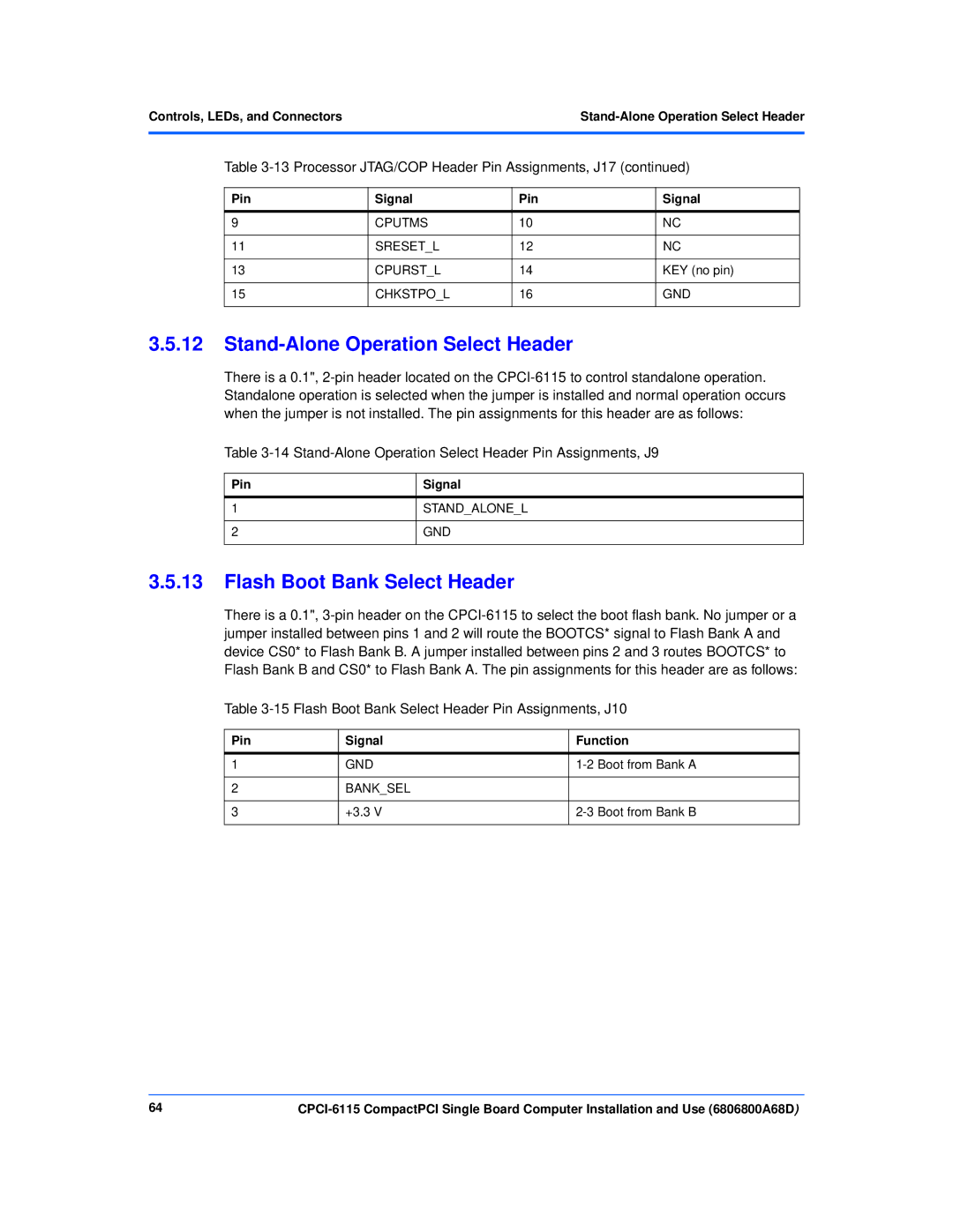
Flash Boot Bank Select Header
15 Flash Boot Bank Select Header Pin Assignments, J10
Stand-Alone Operation Select Header
Bus Mode Select Header
Srom Initialization Enable Header
Safe Start Header
19 Bank a Write Protect Header Pin Assignments, J99
Flash Bank a Write Protect Header
18 +/-12 V Present Header
20 +/-12 V Present Header Pin Assignments, J15
Functional Description
Block Diagram
Functional Description
General Description
Processor Bus Resources
Processor
3 L3 Cache
4 MV64360 System Controller
4.1 MV64360 CPU Bus Interface
4.2 MV64360 DDR Sdram Interface
MV64360 System Controller
4.5 MV64360 Integrated Gigabit Ethernet MACs
4.3 MV64360 32-bit Interface to Devices
4.4 MV64360 Dual PCI/PCI-X Interfaces
Device Bus Parameters
4.6 MV64360 Integrated 2 Megabit Sram
4.7 MV64360 General-Purpose 32-bit Timer/Counters
4.8 MV64360 Watchdog Timer
4.9 MV64360 I2O Message Unit
Interrupt Controller
PCI Bus Arbitration
MV64360 MPP Pin Function Assignments
Board Reset Logic
4.15 MV64360 MPP Configuration
MPP Pin Number Input/Output Function
MPP Pin
4.16 MV64360 Reset Configuration
Functional DescriptionMV64360 System Controller
Input/Output Function
Bus Signal
MV64360 Power-Up Configuration Settings
Default Device AD
Description State of Bit vs. Function
MII/GMII
PCI1 DLL
PCI0 DLL
PCS
System MemoryFunctional Description
System Memory
System Memory Options
Device Organization Memory Device Size Bank Size
Bank a Flash Options
NVRAM, Real-Time Clock, Watchdog Timer
Flash Memory
Flash Bank Size Intel Part Number Device Size
Serial Eeprom Devices
8 TL16C550C Uart Devices
System Registers
PCI Bus
CompactPCI Bus
IDE Controller
Intel 21555 PCI-to-PCI Bridge
PMC Slots
PrPMC Signal Support
Processor PMC Support
PMC Slots
Interrupt Handling
Miscellaneous
Clock Generation
Functional DescriptionMiscellaneous
Interrupt Handling
2.1 MV64360 Interrupt Controller
MV64360 Interrupt Assignments
Edge/L
Machine Check
Sources of Reset
Soft Reset
2.5 SMI
Hot Swap Support
Onboard Power Supplies
Onboard Power Supplies
Hot Swap Process
Intel 21555 Hot Swap Support
Transition Module Preparation and Installation
Block Diagram
Transition Module Preparation and Installation
Preparing the Transition Module
Preparing the Transition Module
On-Board Connectors and Headers
Rear Panel Connectors
CPCI-6115-MCPTM Rear Panel Connectors
Type Number Description
CompactFlash IDE Connector Pin Assignments, J1
IDE CompactFlash Connector
PMC I/O Module Connectors
IDE CompactFlash Connector
Pin J10
Host IO Connectors
PMC I/O Module 1 Host I/O Connector Pin Assignments, J10
IN1DCD
PMC I/O Module 2 Host I/O Connector Pin Assignments, J20
Pin J20
PMC I/O Connectors
LPaDA+ TX1+ LPaDA-TX1
Ethernet
Dioral
Diordya
Serial COM Ports
Mxsyncl
10BaseT/100BaseTx Connector Pin Assignments
5 10/100/1000BaseTx Connectors
6 COM1 And COM2 Connectors MXP Version
10 COM1, COM2 Connector Pin Assignments
7 RJ-45 to DB-9 Adapter for COM1 to PC COM1
11 Wire Interconnection List RJ-45 to DB-9
RF-45 Signal RJ-45 Pin DB-9 Pin DB-9 Signal
RJ-45 to DB-9 Adapter for COM1 to PC COM1
2 COM1 and COM2 Asynchronous Serial Ports Jumpers
Jumper Settings
CompactFlash Jumper
102
Functional Description
IDE Flash
Serial Eeprom
Ethernet Interface CompactPCI Version
Hot-Swap Support
PMC I/O Modules
Asynchronous Serial Ports
6.1 I/O Signal Multiplexing Iomx
12 Multiplexing Sequence of the Iomx Function
RTS3 CTS3 DTR3 DSR3 RTS1 DCD3 RTS2 CTS1
Serial Port Signal Descriptions
106
Asynchronous Serial Port Diagrams
Synchronous Port Board Connector Jumper Header
Serial Port Redirection
Port Configuration Diagrams
PMC I/O Module
108
PMC I/O Module Form Factor
PMC I/O Module Form Factor
PMC I/O Module Presence Detection and Identification
PMC I/O Connector
Host I/O Connector
110
Installing the PIM
Installing the PIM
Installing the PIM
112
Installing the Transition Module
Installing the Transition Module
Removing the Transition Module in a Hot-Swap Chassis
114
Remote Start via the PCI Bus
Register Description
Bit Number Description
Command/Response Register Description
Remote Start via the PCI Bus
116
MOTLoad Firmware
MOTLoad Description
MOTLoad Implementation and Memory Requirements
MOTLoad Tests
MOTLoad Commands
MOTLoad Utility Applications
MOTLoad Firmware
Using MOTLoad
Command Line Interface
Using MOTLoad
MOTLoad FirmwareCommand Line Help
Command Line Help
Command Line Rules
120
MOTLoad Command List
MOTLoad Command List
MOTLoad Commands
Command Description
MOTLoad FirmwareMOTLoad Command List
122
MOTLoad Command ListMOTLoad Firmware
124
Memory Maps
Default Processor Memory Map
Default Processor Memory Map
Memory Maps
Processor Memory Map
Memory MapsProcessor Memory Map
126
Default PCI Memory Map
Default PCI Memory Map
Default PCI Address Map
Suggested PPC Memory Map
Memory MapsSuggested PCI Memory Map
Suggested PCI Memory Map
Suggested PCI Memory Map
128
CompactPCI Memory Map
System I/O Memory Map
PCI Local Bus Memory Map
Device Bank 1 I/O Memory Map
Address Decoding with
9 L1, L2 and L3 Cache
Apollo L3CR Register Assignments
Manufacturers’ Documents
Related Documentation
Embedded Communications Computing Documents
Table A-1 Motorola ECC Documents
Related Specifications
Table A-3 Related Specifications
Related SpecificationsRelated Documentation
MPR-PPC-RPU-02
Related Documentation
134
Index
COM1
136