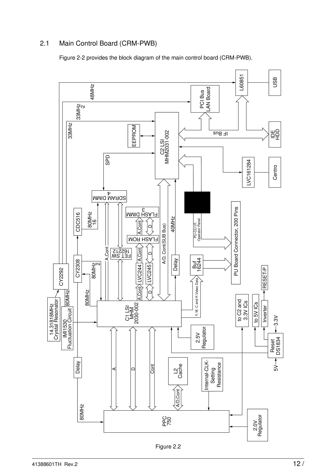
2.1Main Control Board (CRM-PWB)
Figure 2-2 provides the block diagram of the main control board (CRM-PWB).
| 48MHz |
|
|
| 33MHz ·2 |
|
|
33MHz | SPD | EEPROM | C2LSI |
|
|
| ·4 |
|
|
|
|
|
|
| DIMM SDRAM |
|
|
| |||
| CDC516 | 80MHz |
|
| 3 | ⋅ |
|
|
|
|
| A,Cont | D | Bus) | 40MHz | ||
| 16 ⋅ |
|
| |||||
|
|
|
|
| DIMM FLASH | A/D,Cont(SUB |
| |
CY2292 | CY2308 | 80MHz | A,Cont |
| LVC244A,Cont | LVC245 | Delay | |
|
|
|
|
| FLASH MOR |
|
| |
|
|
|
| 162212 | D |
|
| |
|
|
|
| FET SW |
|
|
| |
|
| ⋅2 |
|
|
|
|
|
|
14.31818MHz CrystalResonator | 80MHz | 80MHz |
|
| A,Cont | D |
|
|
IMI1530 FluctuationCircuit |
|
| C1LSI MHM 2030002- |
|
| |||
| Delay |
|
| A | D | Cont |
| L2 Cache |
| 80MHz |
|
|
|
|
| PPC 750 | A/D,Cont |
| PCIBus LANBoard | L60851 |
|
| USB |
| Bus | IF |
|
| IDE HDD |
|
|
|
| ||
|
| LVC161284 |
|
| Centro |
Buf | 16244 | Pins |
|
|
|
OperatorPanel | Connector,200 |
|
|
| |
DataVideo | PUBoard |
|
| ||
Buf | 16244 |
|
|
|
|
Y,M,CandK | toC2and 3.3VICs | to5VICs | Inverter | 3.3V | |
2.5V Regulator |
|
|
| Reset DS1834 | |
|
|
|
| 5V | |
2.0V Regulator
Figure 2.2
41388601TH Rev.2 | 12 / |
