PRELIMINARY
Flash Module Control Registers
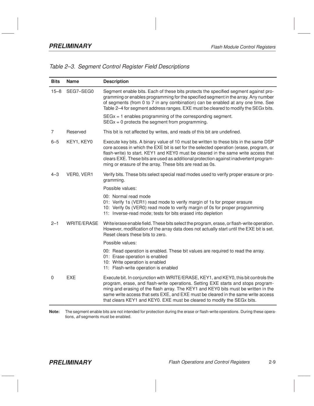
Table 2±3. Segment Control Register Field Descriptions
Bits | Name | Description |
|
|
|
15±8 | SEG7±SEG0 | Segment enable bits. Each of these bits protects the specified segment against pro- |
|
| gramming or enables programming for the specified segment in the array. Any number |
|
| of segments (from 0 to 7 in any combination) can be enabled at any one time. See |
|
| Table 2±4 for segment address ranges. EXE must be cleared to modify the SEGx bits. |
|
| SEGx = 1 enables programming of the corresponding segment. |
|
| SEGx = 0 protects the segment from programming. |
7 | Reserved | This bit is not affected by writes, and reads of this bit are undefined. |
6±5 | KEY1, KEY0 | Execute key bits. A binary value of 10 must be written to these bits in the same DSP |
|
| core access in which the EXE bit is set for the selected operation (erase, program, or |
|
| |
|
| clears EXE. These bits are used as additional protection against inadvertent program- |
|
| ming or erasure of the array. These bits are read as 0s. |
4±3 | VER0, VER1 | Verify bits. These bits select special read modes used to verify proper erasure or pro- |
|
| gramming. |
|
| Possible values: |
|
| 00: Normal read mode |
|
| 01: Verify 1s (VER1) read mode to verify margin of 1s for proper erasure |
|
| 10: Verify 0s (VER0) read mode to verify margin of 0s for proper programming |
|
| 11: |
2±1 | WRITE/ERASE | Write/erase enable field. These bits select the program, erase, or |
|
| However, modification of the array data does not actually start until the EXE bit is set. |
|
| Reset clears these bits to zero. |
|
| Possible values: |
|
| 00: Read operation is enabled. These bit values are required to read the array. |
|
| 01: Erase operation is enabled |
|
| 10: Write operation is enabled |
|
| 11: |
0 | EXE | Execute bit. In conjunction with WRITE/ERASE, KEY1, and KEY0, this bit controls the |
|
| program, erase, and |
|
| ming and erasing of the flash array. The KEY1 and KEY0 bits must be written in the |
|
| same write access that sets EXE, and EXE must be cleared in the same write access |
|
| that clears KEY1 and KEY0. EXE must be cleared to modify the SEGx bits. |
|
| |
Note: | The segment enable bits are not intended for protection during the erase or | |
| tions, all segments must be enabled. | |
PRELIMINARY | Flash Operations and Control Registers |