TMS320F20x/F24x DSP Embedded Flash Memory Technical Reference
Literature Number SPRU282 September
Printed on Recycled Paper
IMPORTANT NOTICE
PRELIMINARY
How to Use This Manual
Read This First
About This Manual
PRELIMINARY
PRELIMINARY
Notational Conventions
This document uses the following conventions
Related Documentation From Texas Instruments
PRELIMINARY
PRELIMINARY
TMS320C2xx C Source Debugger Users Guide literature number SPRU151 tells you how to invoke the C2xx emulator and simulator ver- sions of the C source debugger interface. This book discusses various aspects of the debugger interface, including window management, com- mand entry, code execution, data management, and breakpoints. It also includes a tutorial that introduces basic debugger functionality
PRELIMINARY
PRELIMINARY
North America, South America, Central America
If You Need Assistance
World-Wide Web Sites
Europe, Middle East, Africa
PRELIMINARY
PRELIMINARY
Contents
1 Introduction
2 Flash Operations and Control Registers
A.1.1 Header File for Constants and Variables, SVAR20.H . . . . . . . . . . . . . . . . . . . . . A2 A.1.2 Clear Algorithm, SCLR20.ASM . . . . . . . . . . . . . . . . . . . . . . . . . . . . . . . . . . . . . . . . A5 A.1.3 Erase Algorithm, SERA20.ASM . . . . . . . . . . . . . . . . . . . . . . . . . . . . . . . . . . . . . . A10 A.1.4 Flash-Write Algorithm, SFLW20.ASM . . . . . . . . . . . . . . . . . . . . . . . . . . . . . . . . . A15 A.1.5 Programming Algorithm, SPGM20.ASM . . . . . . . . . . . . . . . . . . . . . . . . . . . . . . . A19 A.1.6 Subroutines Used By All Four Algorithms, SUTILS20.ASM . . . . . . . . . . . . . . . A25
Figures
1±1 TMS320 Devices With On-Chip Flash EEPROM
Tables
2±1 Operations that Modify the Contents of the Flash Array
2±2 Flash Module Control Registers
Page
Introduction
Chapter
Topic
1.1 Basic Concepts of Flash Memory Technology
PRELIMINARY
PRELIMINARY
PRELIMINARY
1.2 TMS320F20x/F24x Flash Module
Table 1±1. TMS320 Devices With On-Chip Flash EEPROM
PRELIMINARY
PRELIMINARY
Figure 1±1. TMS320F20x/F24x Program Space Memory Maps
PRELIMINARY
TMS320F20x/F24x Flash Module
1.3 Benefits of Embedded Flash Memory in a DSP System
PRELIMINARY
PRELIMINARY
PRELIMINARY
PRELIMINARY
Flash Operations and Control Registers
Topic
Page
Chapter
2.1 Operations that Modify the Contents of the F20x/F24x Flash Array
PRELIMINARY
PRELIMINARY
This procedure is discussed in complete detail in Chapter
PRELIMINARY
PRELIMINARY
Operations that Modify the Contents of the F20x/F24x Flash Array
Table 2±1. Operations that Modify the Contents of the Flash Array
Figure 2±1. Flash Memory Logic Levels During Programming and Erasing
PRELIMINARY
2.2 Accessing the Flash Module
PRELIMINARY
PRELIMINARY
PRELIMINARY
Figure 2±2. Memory Maps in Register and Array Access Modes
2.2.1 TMS320F206 Flash Access-Control Register
PRELIMINARY
2.2.2 TMS320F24x Flash Access-Control Register
PRELIMINARY
PRELIMINARY
2.3.1 Segment Control Register SEGCTR
2.3 Flash Module Control Registers
Table 2±2. Flash Module Control Registers
Figure 2±3. Segment Control Register SEGCTR
PRELIMINARY
Table 2±3. Segment Control Register Field Descriptions
PRELIMINARY
Flash Module Control Registers
2.3.3 Write Address Register WADRS
Table 2±4. Flash Array Segments Summary
2.3.2 Flash Test Register TST
PRELIMINARY
2.3.4 Write Data Register WDATA
PRELIMINARY
PRELIMINARY
2.4 Read Modes
PRELIMINARY
PRELIMINARY
2.5 Program Operation
PRELIMINARY
PRELIMINARY
PRELIMINARY
2.6 Erase Operation
PRELIMINARY
Erase Operation
2.7 Recovering From Over-Erasure Flash-Write Operation
PRELIMINARY
PRELIMINARY
PRELIMINARY
2.8 Reading From the Flash Array
2.9 Protecting the Array
PRELIMINARY
PRELIMINARY
Algorithm Implementations and Software Considerations
Chapter
PRELIMINARY
PRELIMINARY
3.1 How the Algorithms Fit Into the Program-Erase-Reprogram Flow
PRELIMINARY
How the Algorithms Fit Into the Program-Erase-Reprogram Flow
PRELIMINARY
Figure 3±1. Algorithms in the Overall Flow
PRELIMINARY
How the Algorithms Fit Into the Program-Erase-Reprogram Flow
PRELIMINARY
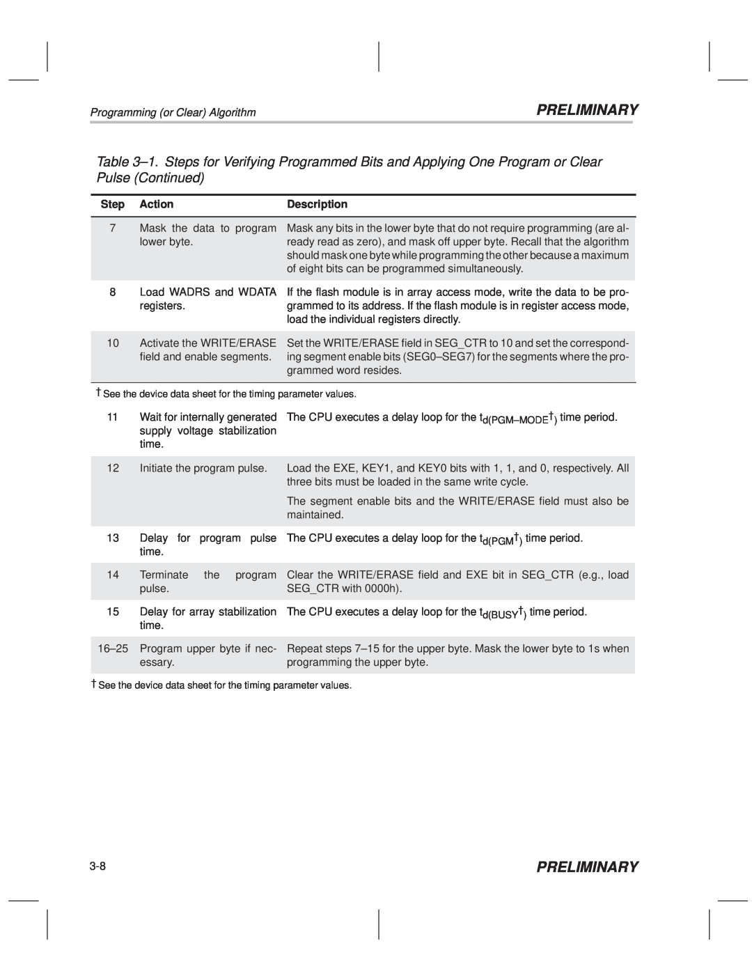
3.2 Programming or Clear Algorithm
Figure 3±2. The Programming Algorithm in the Overall Flow
PRELIMINARY
The main feature of the program/clear algorithm is the concept of program- ming an entire row of bits in a group. The F20x/F24x flash array is organized in rows of 32 words. That is, addresses 0000h through 001Fh are physically located on the same row of the flash memory array. The array is designed so that there is a dependence between the charge levels on adjacent even±odd addresses during programming. Programming the bits of an odd address re- duces the charge margin of the programmed bits the 0s in the preceding ad- jacent even address within the row. Similarly, programming the bits of an even address reduces the charge margin of the programmed bits in the next adjacent odd address within the row. Because of this dependence, if each address is programmed individually, the charge levels among programmed bits is not uniform. The programming algorithm improves the uniformity of charge levels on programmed bits by programming all of the words of a row in a group. For example, the contents of address 0000h is compared with the data to be programmed and one program pulse is applied if necessary. The same procedure is performed on addresses 0001h through 001Fh. The proce- dure repeats starting at address 0000h until no more program pulses are re- quired for any address in the row. The number of iterations of this loop equals the maximum number of program pulses required to program the bits in the row
PRELIMINARY
PRELIMINARY
PRELIMINARY
Figure 3±3. Programming or Clear Algorithm Flow
PRELIMINARY
Programming or Clear Algorithm
Power up the VCCP pin
PRELIMINARY
PRELIMINARY
PRELIMINARY
PRELIMINARY
Programming or Clear Algorithm
Before each program pulse is applied, a read of the byte is performed to deter- mine which bits have reached the programmed level. Any bits that have reached the programmed level are masked set to 1 in the WDATA register. This method of programming provides uniform charge levels among pro- grammed bits, whereas using a single, long program pulse could result in some bits having much more charge than others. The uniformity of charge lev- els among bits has the primary effect of reducing programming time and the secondary effect of reducing the time for a subsequent erase operation. To as- sure that the bits are programmed with enough margin, the reads associated with programming use the VER0 read mode
PRELIMINARY
PRELIMINARY
PRELIMINARY
3.3 Erase Algorithm
Figure 3±4. Erase Algorithm in the Overall Flow
PRELIMINARY
Table 3±2. Steps for Applying One Erase Pulse
PRELIMINARY
PRELIMINARY
4 The actual address is restored
PRELIMINARY
PRELIMINARY
PRELIMINARY
Figure 3±5. Erase Algorithm Flow
PRELIMINARY
Erase Algorithm
PRELIMINARY
3.4 Flash-Write Algorithm
Figure 3±6. Flash-Write Algorithm in the Overall Flow
PRELIMINARY
Table 3±3. Steps for Applying One Flash-Write Pulse
PRELIMINARY
PRELIMINARY
PRELIMINARY
Figure 3±7. Flash-Write Algorithm Flow
PRELIMINARY
Flash-Write Algorithm
The CPU frequency range for the application is an important consideration for the depletion test, as well as for the program and erase operations. Because of the actual implementation of the flash memory circuitry, a bit in depletion mode is most easily detected at low frequency. Accordingly, if the application requires a variable CPU clock rate, the depletion test should be performed at the lowest frequency in the range. Only the read portion of the depletion test must be performed at the lower frequency, because it is the read that is used to detect depletion. The effective duration of the read operation can be ex- tended by sequentially executing multiple reads on the same location. Be- cause the same address is selected the entire time and internal control signals are maintained between reads, the final read is equivalent to a slow read. For example, if the DSP core is executing the programming algorithm at a CLKOUT rate of 20 MHz 50 ns, sequentially reading a location three times is equivalent to reading it once at 6.67 MHz 150 ns. The erase and flash-write algorithm implementations given in Appendix A use three reads to check for depletion
PRELIMINARY
PRELIMINARY
PRELIMINARY
PRELIMINARY
PRELIMINARY
Assembly Source Listings and Program Examples
AppendixAppendixAA
PRELIMINARY
PRELIMINARY
A.1 Assembly Source for Algorithms
A.1.1 Header File for Constants and Variables, SVAR20.H
PRELIMINARY
PRELIMINARY
Assembly Source for Algorithms
Assembly Source Listings and Program Examples
PRELIMINARY
Assembly Source for Algorithms
PRELIMINARY
PRELIMINARY
A.1.2 Clear Algorithm, SCLR20.ASM
PRELIMINARY
PRELIMINARY
Assembly Source for Algorithms
PRELIMINARY
PRELIMINARY
PRELIMINARY
Assembly Source for Algorithms
Assembly Source Listings and Program Examples
PRELIMINARY
Assembly Source for Algorithms
PRELIMINARY
PRELIMINARY
PRELIMINARY
Assembly Source for Algorithms
Assembly Source Listings and Program Examples
PRELIMINARY
PRELIMINARY
A.1.3 Erase Algorithm, SERA20.ASM
PRELIMINARY
A-10
PRELIMINARY
Assembly Source for Algorithms
Assembly Source Listings and Program Examples
PRELIMINARY
PRELIMINARY
Assembly Source for Algorithms
PRELIMINARY
A-12
PRELIMINARY
Assembly Source for Algorithms
Assembly Source Listings and Program Examples
PRELIMINARY
PRELIMINARY
Assembly Source for Algorithms
PRELIMINARY
A-14
A.1.4 Flash-Write Algorithm, SFLW20.ASM
PRELIMINARY
PRELIMINARY
PRELIMINARY
Assembly Source for Algorithms
PRELIMINARY
A-16
PRELIMINARY
Assembly Source for Algorithms
Assembly Source Listings and Program Examples
PRELIMINARY
PRELIMINARY
Assembly Source for Algorithms
PRELIMINARY
A-18
A.1.5 Programming Algorithm, SPGM20.ASM
PRELIMINARY
PRELIMINARY
PRELIMINARY
Assembly Source for Algorithms
PRELIMINARY
A-20
PRELIMINARY
Assembly Source for Algorithms
Assembly Source Listings and Program Examples
PRELIMINARY
PRELIMINARY
Assembly Source for Algorithms
PRELIMINARY
A-22
PRELIMINARY
Assembly Source for Algorithms
Assembly Source Listings and Program Examples
PRELIMINARY
PRELIMINARY
Assembly Source for Algorithms
PRELIMINARY
A-24
Assembly Source Listings and Program Examples
A.1.6 Subroutines Used By All Four Algorithms, SUTILS20.ASM
Assembly Source for Algorithms
PRELIMINARY
PRELIMINARY
Assembly Source for Algorithms
PRELIMINARY
A-26
PRELIMINARY
A.2 C-Callable Interface to Flash Algorithms
Assembly Source Listings and Program Examples
PRELIMINARY
C-Callable Interface to Flash Algorithms
PRELIMINARY
PRELIMINARY
A-28
PRELIMINARY
Assembly Source Listings and Program Examples
PRELIMINARY
C-Callable Interface to Flash Algorithms
C-Callable Interface to Flash Algorithms
PRELIMINARY
PRELIMINARY
A-30
PRELIMINARY
Assembly Source Listings and Program Examples
PRELIMINARY
C-Callable Interface to Flash Algorithms
PRELIMINARY
A.3 Sample Assembly Code to Erase and Reprogram the TMS320F206
A.3.1 Assembly Code for TMS320F206
PRELIMINARY
PRELIMINARY
PRELIMINARY
PRELIMINARY
PRELIMINARY
A-34
PRELIMINARY
Sample Assembly Code to Erase and Reprogram the TMS320F206
Assembly Source Listings and Program Examples
PRELIMINARY
PRELIMINARY
Sample Assembly Code to Erase and Reprogram the TMS320F206
PRELIMINARY
A-36
A.4 Sample C Code to Erase and Reprogram the TMS320F206
PRELIMINARY
PRELIMINARY
PRELIMINARY
A.4.2 Linker Command File for TMS320F206 Sample C Code
PRELIMINARY
Sample C Code to Erase and Reprogram the TMS320F206
PRELIMINARY
Assembly Source Listings and Program Examples
PRELIMINARY
Sample C Code to Erase and Reprogram the TMS320F206
PRELIMINARY
A.5 Sample Assembly Code to Erase and Reprogram the TMS320F240
A.5.1 Assembly Code for TMS320F240
PRELIMINARY
PRELIMINARY
Sample Assembly Code to Erase and Reprogram the TMS320F240
Assembly Source Listings and Program Examples
PRELIMINARY
PRELIMINARY
Sample Assembly Code to Erase and Reprogram the TMS320F240
PRELIMINARY
A-42
PRELIMINARY
Sample Assembly Code to Erase and Reprogram the TMS320F240
Assembly Source Listings and Program Examples
PRELIMINARY
PRELIMINARY
Sample Assembly Code to Erase and Reprogram the TMS320F240
PRELIMINARY
A-44
Assembly Source Listings and Program Examples
A.5.2 Linker Command File for TMS320F240 Sample Assembly Code
Sample Assembly Code to Erase and Reprogram the TMS320F240
PRELIMINARY
PRELIMINARY
Sample Assembly Code to Erase and Reprogram the TMS320F240
PRELIMINARY
A-46
PRELIMINARY
A.6 Using the Algorithms With C Code to Erase and Reprogram the F240
PRELIMINARY
Rev1.003/98 JGC
PRELIMINARY
A.6.2 Linker Command File for TMS320F240 Sample C Code
Using the Algorithms With C Code to Erase and Reprogram the F240
PRELIMINARY
PRELIMINARY
Using the Algorithms With C Code to Erase and Reprogram the F240
Assembly Source Listings and Program Examples
PRELIMINARY
PRELIMINARY
A.6.3 C Function for Disabling TMS320F240 Watchdog Timer
Using the Algorithms With C Code to Erase and Reprogram the F240
PRELIMINARY
Assembly Source Listings and Program Examples
A.6.4 C Functions for Initializing the TMS320F240
Using the Algorithms With C Code to Erase and Reprogram the F240
PRELIMINARY
PRELIMINARY
Using the Algorithms With C Code to Erase and Reprogram the F240
PRELIMINARY
A-52
PRELIMINARY
Index
PRELIMINARY
Index
PRELIMINARY
PRELIMINARY
Index
PRELIMINARY
PRELIMINARY
Index
PRELIMINARY
PRELIMINARY
Index