PRELIMINARY
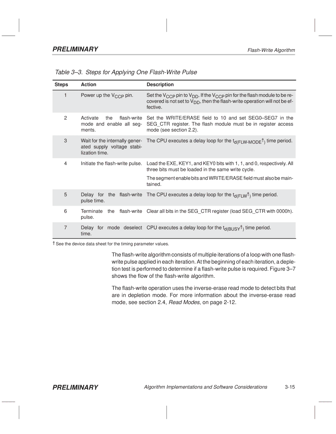
Table 3±3. Steps for Applying One Flash-Write Pulse
Steps | Action | Description |
1 Power up the VCCP pin.
Set the VCCP pin to VDD. If the VCCP pin for the flash module to be re- covered is not set to VDD, then the
fective.
2Activate the
3Wait for the internally gener- ated supply voltage stabi- lization time.
Set the WRITE/ERASE field to 10 and set SEG0±SEG7 in the SEG_CTR register. The flash module must be in register access mode (see section 2.2).
The CPU executes a delay loop for the
4Initiate the
The segment enable bits and WRITE/ERASE field must also be main- tained.
5 | Delay | for | the | The CPU executes a delay loop for the t | ² | time period. |
| pulse time. |
|
| d(FLW ) |
| |
|
|
|
|
| ||
|
|
| ||||
6 | Terminate the | Clear all bits in the SEG_CTR register (load SEG_CTR with 0000h). | ||||
| pulse. |
|
|
|
|
|
|
|
|
|
| ||
7 | Delay | for | mode deselect | CPU executes a delay loop for the td(BUSY² ) time period. | ||
| time. |
|
|
|
|
|
|
|
|
|
|
|
|
²See the device data sheet for the timing parameter values.
The
The
PRELIMINARY | Algorithm Implementations and Software Considerations |