Flash Module Control Registers
PRELIMINARY
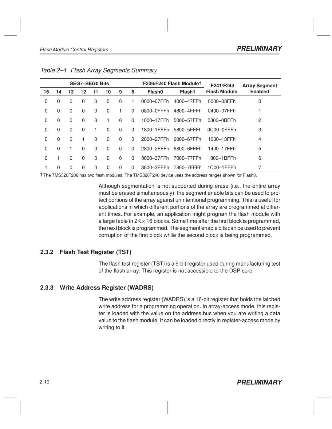
Table 2±4. Flash Array Segments Summary
|
| SEG7±SEG0 Bits |
|
| 'F206/F240 Flash Module² | 'F241/F243 | Array Segment | ||||
15 | 14 | 13 | 12 | 11 | 10 | 9 | 8 | Flash0 | Flash1 | Flash Module | Enabled |
|
|
|
|
|
|
|
|
|
|
|
|
0 | 0 | 0 | 0 | 0 | 0 | 0 | 1 | 0000±07FFh | 4000±47FFh | 0000±03FFh | 0 |
0 | 0 | 0 | 0 | 0 | 0 | 1 | 0 | 0800±0FFFh | 4800±4FFFh | 0400±07FFh | 1 |
0 | 0 | 0 | 0 | 0 | 1 | 0 | 0 | 1000±17FFh | 5000±57FFh | 0800±0BFFh | 2 |
0 | 0 | 0 | 0 | 1 | 0 | 0 | 0 | 1800±1FFFh | 5800±5FFFh | 0C00±0FFFh | 3 |
0 | 0 | 0 | 1 | 0 | 0 | 0 | 0 | 2000±27FFh | 6000±67FFh | 1000±13FFh | 4 |
0 | 0 | 1 | 0 | 0 | 0 | 0 | 0 | 2800±2FFFh | 6800±6FFFh | 1400±17FFh | 5 |
0 | 1 | 0 | 0 | 0 | 0 | 0 | 0 | 3000±37FFh | 7000±77FFh | 1800±1BFFh | 6 |
1 | 0 | 0 | 0 | 0 | 0 | 0 | 0 | 3800±3FFFh | 7800±7FFFh | 1C00±1FFFh | 7 |
²The TMS320F206 has two flash modules. The TMS320F240 device uses the address ranges shown for Flash0.
Although segmentation is not supported during erase (i.e., the entire array must be erased simultaneously), the segment enable bits can be used to pro- tect portions of the array against unintentional programming. This is useful for applications in which different portions of the array are programmed at differ- ent times. For example, an application might program the flash module with a large table in 2K ×16 blocks. Some time after the first block is programmed, the next block is programmed. The segment enable bits can be used to prevent corruption of the first block while the second block is being programmed.
2.3.2Flash Test Register (TST)
The flash test register (TST) is a
2.3.3Write Address Register (WADRS)
The write address register (WADRS) is a
PRELIMINARY |
