Literature Number SPRU282 September
Important Notice
Read This First
Preliminary
Related Documentation From Texas Instruments
Preliminary
If You Need Assistance
Viii
Contents
Contents
Figures
Tables
Introduction
Basic Concepts of Flash Memory Technology
TMS320F20x/F24x Flash Module
±1. TMS320 Devices With On-Chip Flash Eeprom
±1. TMS320F20x/F24x Program Space Memory Maps
Benefits of Embedded Flash Memory in a DSP System
Preliminary
Flash Operations and Control Registers
Topic
Preliminary
Flash Operations and Control Registers
±1. Flash Memory Logic Levels During Programming and Erasing
Accessing the Flash Module
±2. Memory Maps in Register and Array Access Modes
1 TMS320F206 Flash Access-Control Register
2 TMS320F24x Flash Access-Control Register
OUT
Flash Module Control Registers
Segment Control Register Segctr
±3. Segment Control Register Field Descriptions
Flash Test Register TST
Write Address Register Wadrs
Write Data Register Wdata
Read Modes
Program Operation
Erase Operation
Recovering From Over-Erasure Flash-Write Operation
Reading From the Flash Array
Protecting the Array
Algorithm Implementations Software Considerations
How the Algorithms Fit Into the Program-Erase-Reprogram Flow
±1. Algorithms in the Overall Flow
Programming or Clear Algorithm
±2. The Programming Algorithm in the Overall Flow
Preliminary
±3. Programming or Clear Algorithm Flow
Step Action Description
Mask the data to program
Preliminary
Erase Algorithm
±4. Erase Algorithm in the Overall Flow
±2. Steps for Applying One Erase Pulse
Preliminary
±5. Erase Algorithm Flow
Flash-Write Algorithm
±6. Flash-Write Algorithm in the Overall Flow
±3. Steps for Applying One Flash-Write Pulse
±7. Flash-Write Algorithm Flow
Preliminary
Preliminary
Assembly Source Listings Program Examples
Assembly Source for Algorithms
Header File for Constants and Variables, SVAR20.H
BASE+0
Error
BASE0
BASE1
D7K
Constants
D5K
Dloop
Segend
Clear Algorithm, SCLR20.ASM
Segst
Protect
AR0
Gclr PROTECT,SEGST,SEGEND DELAY,REGS,ARRAY
Splk #0,ERROR
AR1
Lacl Fladrs
Exit Splk #1,ERROR
Sacl Flst
Newrow
Shutdown Write Operation Tblw SPAD1 Execute Command LAR
Activate Write BIT Tblw SPAD1 Execute Command LAR
SET Delay Call DELAY,*,AR6 Wait Stop Write Operation Splk
Tblr Fldata
Lacl BASE2
Tblw SPAD1 Execute Command LAR
Prgbyte Call SETRDVER0
Bcnd PBDONE,EQ
Erase Algorithm, SERA20.ASM
Inverse Erase Command Word
Erase Command Word
Erase Exebin Command Word
Flash Write Command Word
Call Setmode
Clrc OVM
Sacl Flend
Xorerase
Bldd
Splk #STOP,BASE0
Inverase Splk #INVER,BASE0 Call Setmode
Nextivers Lacl BASE1
Flash Stop command, and Ffff for Wdata
Flash-Write Algorithm, SFLW20.ASM
Bldd #FLST,BASE1
Maxflw
Flws
Bcnd
Call Array Access Flash Array Done
Call DELAY,*,AR6
Flwrite Splk
LAR AR0,#MAXFLW Cmpr
Setmode Call Lacl Tblw LAR Call Call RET
Programming Algorithm, SPGM20.ASM
AR4
PROTECT,DELAY,REGS,ARRAY
AR3
Gpgmj
Mask ALL Interrupts
Setc Intm Globally Mask ALL Interrupts Splk #0,ERROR
Gpgmj Splk
SUB Sacl BASE4
Lacl Fladrs Newrow
Rowdone Lacl Fladrs
Bcnd DONE, GT
Adjrow NEG
Shut Down Write Operation Tblw SPAD1 Execute Command LAR
SETRDVER0 Call Regs Access Flash Registers
Pbend RET
XOR Fldata
Bcnd PBEND,EQ
Subroutines Used By All Four Algorithms, SUTILS20.ASM
OUT SPAD2,F24XACCS
OUT SPAD2,FACCESS0
SPAD2,FACCESS1
Lacc Flst SUB
Callable Interface to Flash Algorithms
PARMS+1
Gclr
SEGST,SEGEND,PROTECT
PARMS+2
Arstack
Lacl Error
Ersparams
Arprotect
LAR AR1,SVAR1
Sacl Erscount
Call Flws
1PROTECT
Popd *+
Call Gpgmj
Sample Assembly Code to Erase and Reprogram the TMS320F206
Assembly Code for TMS320F206
PARMS+1
SUB
Memory
Psaram
Block B2
Sections
DLY Psaram
Sample C Code to Erase and Reprogram the TMS320F206
Linker Command File for TMS320F206 Sample C Code
BLKB2
FLASH0
FLASH1
Block B2 Dsaram
Sample Assembly Code to Erase and Reprogram the TMS320F240
Assembly Code for TMS320F240
CKCR0
Rticr
Wdcr
CKCR1
Sacl Syssr
LDP #DPPF1
PORRST, PLLRST, Illrst SWRST, Wdrst Lacl Syssr Accl = Syssr
LDP #PARMS Splk
Daram
LDP #PARMS
B0PGM
Linker Command File for TMS320F240 Sample Assembly Code
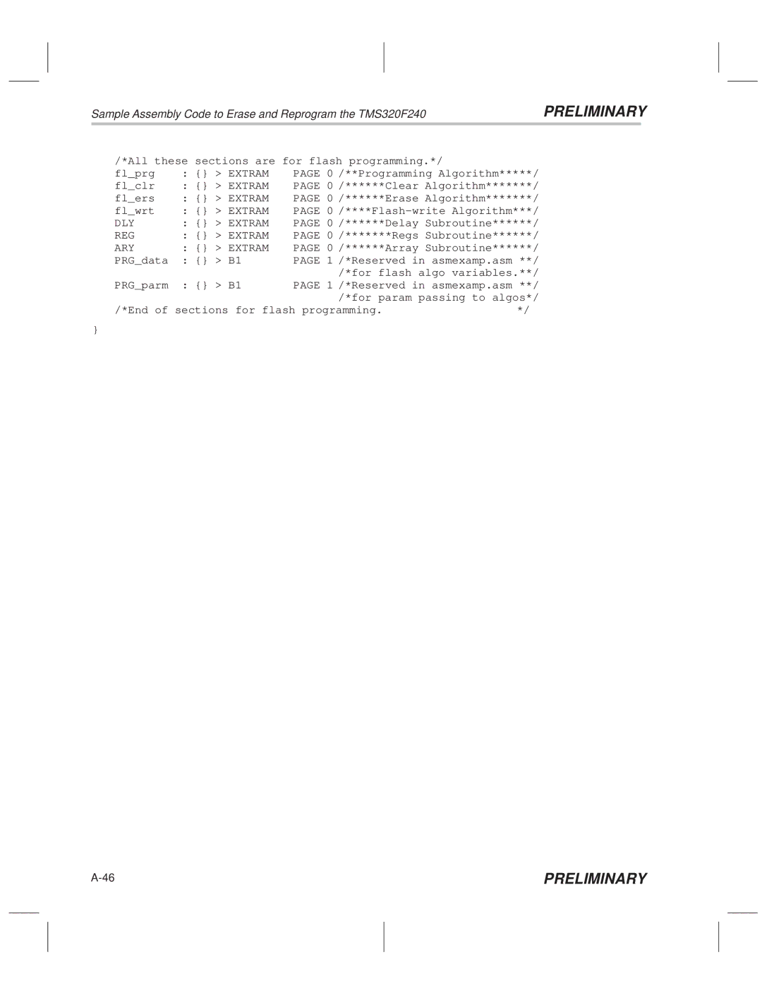
Extram
Extram 0 /******Delay Subroutine
Rev1.003/98 JGC
Linker Command File for TMS320F240 Sample C Code
Block B2 Dsram
B0DAT
Lacl Wdcr
Function for Disabling TMS320F240 Watchdog Timer
Compute Length
Pshd
Functions for Initializing the TMS320F240
Sacl Wdcr
Syscr
Sacl Wdtcr
Index
Assembly code SERA2x.ASM Described 10 to
Margin
Role in single program pulse WRITE/ERASE field Described

