CYV15G0404DXB
Pin Definitions (continued)
CYV15G0404DXB Quad HOTLink II Transceiver
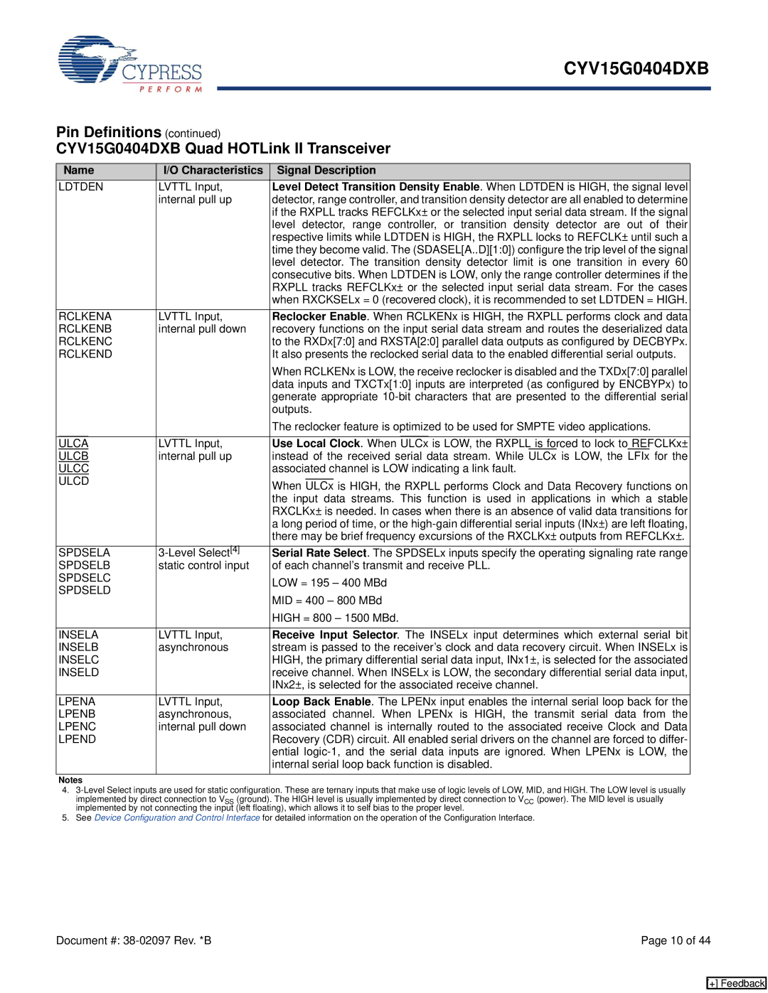
| Name | I/O Characteristics | Signal Description | |||||||
| LDTDEN | LVTTL Input, | Level Detect Transition Density Enable. When LDTDEN is HIGH, the signal level | |||||||
|
|
| internal pull up | detector, range controller, and transition density detector are all enabled to determine | ||||||
|
|
|
| if the RXPLL tracks REFCLKx± or the selected input serial data stream. If the signal | ||||||
|
|
|
| level detector, range controller, or transition density detector are out of their | ||||||
|
|
|
| respective limits while LDTDEN is HIGH, the RXPLL locks to REFCLK± until such a | ||||||
|
|
|
| time they become valid. The (SDASEL[A..D][1:0]) configure the trip level of the signal | ||||||
|
|
|
| level detector. The transition density detector limit is one transition in every 60 | ||||||
|
|
|
| consecutive bits. When LDTDEN is LOW, only the range controller determines if the | ||||||
|
|
|
| RXPLL tracks REFCLKx± or the selected input serial data stream. For the cases | ||||||
|
|
|
| when RXCKSELx = 0 (recovered clock), it is recommended to set LDTDEN = HIGH. | ||||||
| RCLKENA | LVTTL Input, | Reclocker Enable. When RCLKENx is HIGH, the RXPLL performs clock and data | |||||||
| RCLKENB | internal pull down | recovery functions on the input serial data stream and routes the deserialized data | |||||||
| RCLKENC |
| to the RXDx[7:0] and RXSTA[2:0] parallel data outputs as configured by DECBYPx. | |||||||
| RCLKEND |
| It also presents the reclocked serial data to the enabled differential serial outputs. | |||||||
|
|
|
| When RCLKENx is LOW, the receive reclocker is disabled and the TXDx[7:0] parallel | ||||||
|
|
|
| data inputs and TXCTx[1:0] inputs are interpreted (as configured by ENCBYPx) to | ||||||
|
|
|
| generate appropriate | ||||||
|
|
|
| outputs. | ||||||
|
|
|
| The reclocker feature is optimized to be used for SMPTE video applications. | ||||||
|
|
|
|
|
|
| ||||
| ULCA |
| LVTTL Input, | Use Local Clock. When | ULCx | is LOW, the RXPLL is forced to lock to REFCLKx± | ||||
| ULCB | internal pull up | instead of the received serial data stream. While | ULCx | is LOW, the LFIx for the | |||||
| ULCC |
| associated channel is LOW indicating a link fault. | |||||||
| ULCD |
|
|
|
|
|
|
|
| |
|
| When ULCx is HIGH, the RXPLL performs Clock and Data Recovery functions on | ||||||||
|
|
|
| the input data streams. This function is used in applications in which a stable | ||||||
|
|
|
| RXCLKx± is needed. In cases when there is an absence of valid data transitions for | ||||||
|
|
|
| a long period of time, or the | ||||||
|
|
|
| there may be brief frequency excursions of the RXCLKx± outputs from REFCLKx±. | ||||||
| SPDSELA | Serial Rate Select. The SPDSELx inputs specify the operating signaling rate range | ||||||||
| SPDSELB | static control input | of each channel’s transmit and receive PLL. | |||||||
| SPDSELC |
| LOW = 195 – 400 MBd | |||||||
| SPDSELD |
| ||||||||
|
| MID = 400 – 800 MBd | ||||||||
|
|
|
| |||||||
|
|
|
| HIGH = 800 – 1500 MBd. | ||||||
|
|
|
| |||||||
| INSELA | LVTTL Input, | Receive Input Selector. The INSELx input determines which external serial bit | |||||||
| INSELB | asynchronous | stream is passed to the receiver’s clock and data recovery circuit. When INSELx is | |||||||
| INSELC |
| HIGH, the primary differential serial data input, INx1±, is selected for the associated | |||||||
| INSELD |
| receive channel. When INSELx is LOW, the secondary differential serial data input, | |||||||
|
|
|
| INx2±, is selected for the associated receive channel. | ||||||
| LPENA | LVTTL Input, | Loop Back Enable. The LPENx input enables the internal serial loop back for the | |||||||
| LPENB | asynchronous, | associated channel. When LPENx is HIGH, the transmit serial data from the | |||||||
| LPENC | internal pull down | associated channel is internally routed to the associated receive Clock and Data | |||||||
| LPEND |
| Recovery (CDR) circuit. All enabled serial drivers on the channel are forced to differ- | |||||||
|
|
|
| ential | ||||||
|
|
|
| internal serial loop back function is disabled. | ||||||
| Notes |
|
|
|
|
|
|
|
| |
4.
5.See Device Configuration and Control Interface for detailed information on the operation of the Configuration Interface.
Document #: | Page 10 of 44 |
[+] Feedback