CYV15G0404DXB
Transmit Modes
Encoder Bypass
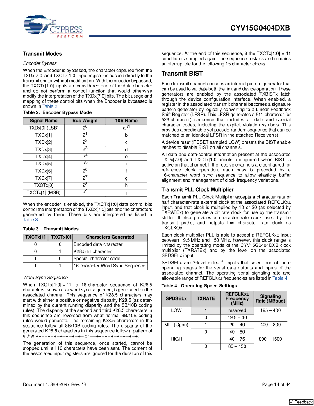
When the Encoder is bypassed, the character captured from the TXDx[7:0] and TXCTx[1:0] input register is passed directly to the transmit shifter without modification. With the encoder bypassed, the TXCTx[1:0] inputs are considered part of the data character and do not perform a control function that would otherwise modify the interpretation of the TXDx[7:0] bits. The bit usage and mapping of these control bits when the Encoder is bypassed is shown in Table 2.
Table 2. Encoder Bypass Mode
Signal Name | Bus Weight | 10B Name |
TXDx[0] (LSB) | 20 | a[7] |
TXDx[1] | 21 | b |
TXDx[2] | 22 | c |
TXDx[3] | 23 | d |
TXDx[4] | 24 | e |
TXDx[5] | 25 | i |
TXDx[6] | 26 | f |
TXDx[7] | 27 | g |
TXCTx[0] | 28 | h |
TXCTx[1] (MSB) | 29 | j |
When the encoder is enabled, the TXCTx[1:0] data control bits control the interpretation of the TXDx[7:0] bits and the characters generated by them. These bits are interpreted as listed in Table 3.
Table 3. Transmit Modes
TXCTx[1] | TXCTx[0] | Characters Generated |
0 | 0 | Encoded data character |
|
|
|
0 | 1 | K28.5 fill character |
|
|
|
1 | 0 | Special character code |
|
|
|
1 | 1 | |
|
|
|
Word Sync Sequence
When TXCTx[1:0] = 11, a
The generation of this sequence, once started, cannot be stopped until all 16 characters have been sent. The content of the associated input registers are ignored for the duration of this
sequence. At the end of this sequence, if the TXCTx[1:0] = 11 condition is sampled again, the sequence restarts and remains uninterruptible for the following 15 character clocks.
Transmit BIST
Each transmit channel contains an internal pattern generator that can be used to validate both the link and device operation. These generators are enabled by the associated TXBISTx latch through the device configuration interface. When enabled, a register in the associated transmit channel becomes a signature pattern generator by logically converting to a Linear Feedback Shift Register (LFSR). This LFSR generates a
A device reset (RESET sampled LOW) presets the BIST enable latches to disable BIST on all channels.
All data and
Transmit PLL Clock Multiplier
Each Transmit PLL Clock Multiplier accepts a character rate or half
Each clock multiplier PLL is able to accept a REFCLKx± input between 19.5 MHz and 150 MHz, however, this clock range is limited by the operating mode of the CYV15G0404DXB clock multiplier (TXRATEx) and by the level on the associated SPDSELx input.
SPDSELx are
Table 4. Operating Speed Settings
|
| REFCLKx± | Signaling | |
SPDSELx | TXRATE | Frequency | ||
Rate (MBaud) | ||||
|
| (MHz) | ||
|
|
| ||
LOW | 1 | reserved | 195 – 400 | |
| 0 | 19.5 – 40 |
| |
|
|
|
| |
MID (Open) | 1 | 20 – 40 | 400 – 800 | |
|
|
|
| |
| 0 | 40 – 80 |
| |
|
|
|
| |
HIGH | 1 | 40 – 75 | 800 – 1500 | |
|
|
|
| |
| 0 | 80 – 150 |
| |
|
|
|
|
Document #: | Page 14 of 44 |
[+] Feedback
