CYV15G0404DXB
CYV15G0404DXB DC Electrical Characteristics (continued)
Parameter |
| Description |
|
| Test Conditions |
| Min. |
| Max. | Unit | |||||||||||||||
Differential | CML Serial Outputs: OUTA1±, OUTA2±, OUTB1±, OUTB2±, OUTC1±, OUTC2±, OUTD1±, OUTD2± |
| |||||||||||||||||||||||
|
|
|
|
|
|
|
|
|
|
|
|
|
|
|
|
|
|
|
|
|
|
|
| ||
VOHC | Output HIGH Voltage |
| 100Ω differential load |
| VCC – 0.5 |
| VCC – 0.2 | V | |||||||||||||||||
| (Vcc Referenced) |
|
|
|
|
|
|
|
|
|
|
| |||||||||||||
|
| Ω | differential load |
| VCC – 0.5 |
| VCC – 0.2 | V | |||||||||||||||||
|
|
|
|
|
|
|
|
|
|
|
|
|
|
|
| 150 |
|
| |||||||
VOLC | Output LOW Voltage |
| 100Ω differential load |
| VCC – 1.4 |
| VCC – 0.7 | V | |||||||||||||||||
| (VCC Referenced) |
|
|
|
|
|
|
|
|
|
|
| |||||||||||||
|
| Ω | differential load |
| VCC – 1.4 |
| VCC – 0.7 | V | |||||||||||||||||
|
|
|
|
|
|
|
|
|
|
|
|
|
|
|
| 150 |
|
| |||||||
VODIF | Output Differential Voltage |
| 100Ω differential load |
| 450 |
| 900 | mV | |||||||||||||||||
| (OUT+) − (OUT−) |
|
|
|
|
|
|
|
|
|
|
| |||||||||||||
|
| 150Ω differential load |
| 560 |
| 1000 | mV | ||||||||||||||||||
|
|
|
|
|
|
|
|
|
|
|
|
|
|
|
|
|
| ||||||||
|
|
|
|
|
|
|
|
|
|
|
|
|
|
|
|
|
|
|
|
| |||||
Differential | Serial Line Receiver Inputs: INA1±, INA2±, | INB1±, INB2±, INC1±, INC2±, IND1±, IND2± |
|
|
| ||||||||||||||||||||
VDIFFs[13] | Input Differential Voltage (IN+) − (IN−) |
|
|
|
|
| 100 |
| 1200 | mV | |||||||||||||||
VIHE | Highest Input HIGH Voltage |
|
|
|
|
|
|
|
|
| VCC | V | |||||||||||||
VILE | Lowest Input LOW Voltage |
|
|
|
|
|
| VCC – 2.0 |
|
| V | ||||||||||||||
IIHE | Input HIGH Current |
| VIN = VIHE Max. |
|
|
|
| 1350 | μA | ||||||||||||||||
IILE | Input LOW Current |
| VIN = VILE Min. |
|
|
| μA | ||||||||||||||||||
VICOM[15] | Common Mode input range |
| ((VCC – 2.0V) + 0.5)min, |
| +1.25 |
| +3.1 | V | |||||||||||||||||
|
|
|
|
|
|
|
|
|
|
|
|
|
|
|
| (VCC | – 0.5V) max. |
|
|
|
|
|
| ||
Power Supply |
|
|
|
|
|
|
|
|
|
|
|
|
|
|
|
|
|
|
| Typ. |
| Max. |
| ||
ICC [16, 17] | Max Power Supply Current |
| REFCLKx = | Commercial |
| 910 |
| 1270 | mA | ||||||||||||||||
|
|
|
|
|
|
|
|
|
|
|
|
|
|
|
| MAX |
|
|
|
|
|
|
|
|
|
|
|
|
|
|
|
|
|
|
|
|
|
|
|
|
|
| Industrial |
|
|
|
| 1320 | mA | ||
|
|
|
|
|
|
|
|
|
|
|
|
|
|
|
|
|
|
|
|
|
| ||||
|
|
|
|
|
|
|
|
|
|
|
|
|
|
|
|
|
|
|
|
|
|
|
| ||
ICC [16, 17] | Typical Power Supply Current |
| REFCLKx = | Commercial |
| 900 |
| 1270 | mA | ||||||||||||||||
|
|
|
|
|
|
|
|
|
|
|
|
|
|
|
| 125 MHz |
|
|
|
|
|
|
|
| |
|
|
|
|
|
|
|
|
|
|
|
|
|
|
|
| Industrial |
|
|
|
| 1320 | mA | |||
|
|
|
|
|
|
|
|
|
|
|
|
|
|
|
|
|
|
|
|
|
| ||||
|
|
|
|
|
|
|
|
|
|
|
|
|
|
|
|
|
|
|
|
|
|
|
|
| |
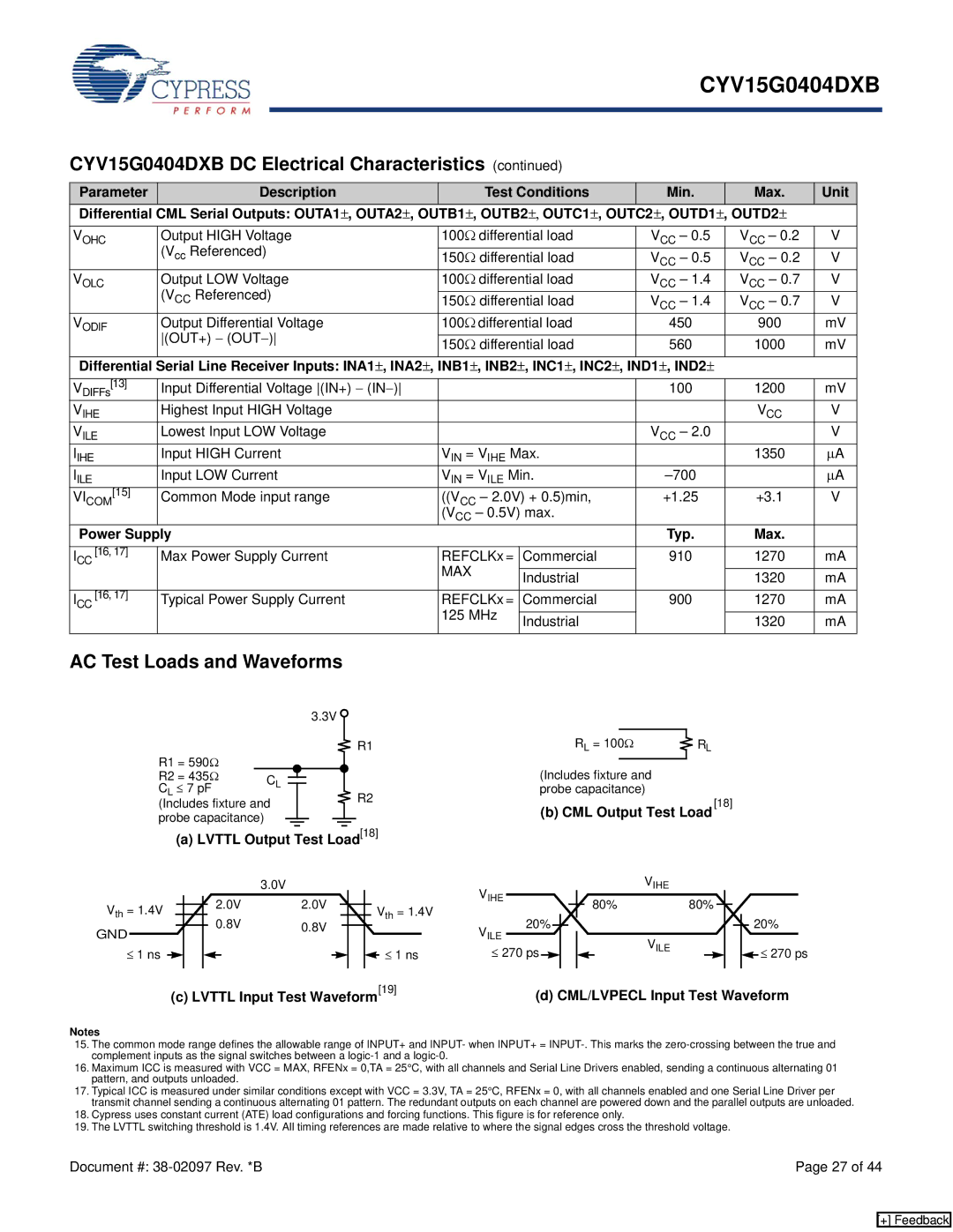
AC Test Loads and Waveforms |
|
|
|
|
|
|
|
|
|
|
| ||||||||||||||
|
|
|
|
|
|
|
|
| 3.3V |
|
|
|
|
|
|
|
|
|
|
|
|
|
| ||
|
|
|
|
|
|
|
|
|
|
|
|
|
| ||||||||||||
|
|
|
|
|
|
|
|
|
|
|
|
|
|
|
|
|
|
|
|
|
|
|
|
| |
| R1 = 590Ω |
|
|
|
|
|
|
|
|
|
|
|
|
| R1 |
|
| RL = 100Ω |
| RL |
|
|
| ||
|
|
|
|
|
|
|
|
|
|
|
|
|
|
|
|
|
|
|
| ||||||
|
|
|
|
|
|
|
|
|
|
|
|
|
|
|
|
|
|
|
| ||||||
|
|
|
|
|
|
|
|
|
|
|
|
|
|
|
|
|
|
|
|
|
|
|
|
| |
|
|
|
|
|
|
|
|
|
|
|
|
|
|
|
|
| (Includes fixture and |
|
|
| |||||
| R2 = 435Ω | CL |
|
|
|
|
|
|
|
|
|
|
|
|
|
|
|
|
| ||||||
|
|
|
|
|
|
|
|
|
|
|
|
|
|
|
|
|
| ||||||||
| CL ≤ 7 pF |
|
|
|
|
| R2 |
|
| probe capacitance) |
|
|
|
|
| ||||||||||
|
|
|
|
|
|
|
|
|
|
|
|
| |||||||||||||
|
|
|
|
|
|
|
|
|
|
|
|
|
|
|
|
|
|
|
|
| |||||
| (Includes fixture and |
|
|
|
|
|
|
|
|
|
|
| (b) CML Output Test Load | [18] |
| ||||||||||
|
|
|
|
|
|
|
|
| |||||||||||||||||
| probe capacitance) |
|
|
|
|
|
|
|
|
|
|
|
|
|
|
|
|
|
| ||||||
|
|
|
|
|
|
|
|
|
|
|
|
|
|
|
|
|
| ||||||||
(a) LVTTL Output Test Load[18]
Vth = 1.4V
GND
≤ 1 ns
3.0V
2.0V 2.0V
0.8V 0.8V
VIHE
Vth = 1.4V
20%
VILE
≤ 1 ns | ≤ 270 ps |
VIHE
80%80%
VILE
20%
![]() ≤ 270 ps
≤ 270 ps
(c) LVTTL Input Test Waveform[19] | (d) CML/LVPECL Input Test Waveform |
Notes
15.The common mode range defines the allowable range of INPUT+ and INPUT- when INPUT+ =
16.Maximum ICC is measured with VCC = MAX, RFENx = 0,TA = 25°C, with all channels and Serial Line Drivers enabled, sending a continuous alternating 01 pattern, and outputs unloaded.
17.Typical ICC is measured under similar conditions except with VCC = 3.3V, TA = 25°C, RFENx = 0, with all channels enabled and one Serial Line Driver per transmit channel sending a continuous alternating 01 pattern. The redundant outputs on each channel are powered down and the parallel outputs are unloaded.
18.Cypress uses constant current (ATE) load configurations and forcing functions. This figure is for reference only.
19.The LVTTL switching threshold is 1.4V. All timing references are made relative to where the signal edges cross the threshold voltage.
Document #: | Page 27 of 44 |
[+] Feedback