CYV15G0404DXB
Pin Definitions (continued)
CYV15G0404DXB Quad HOTLink II Transceiver
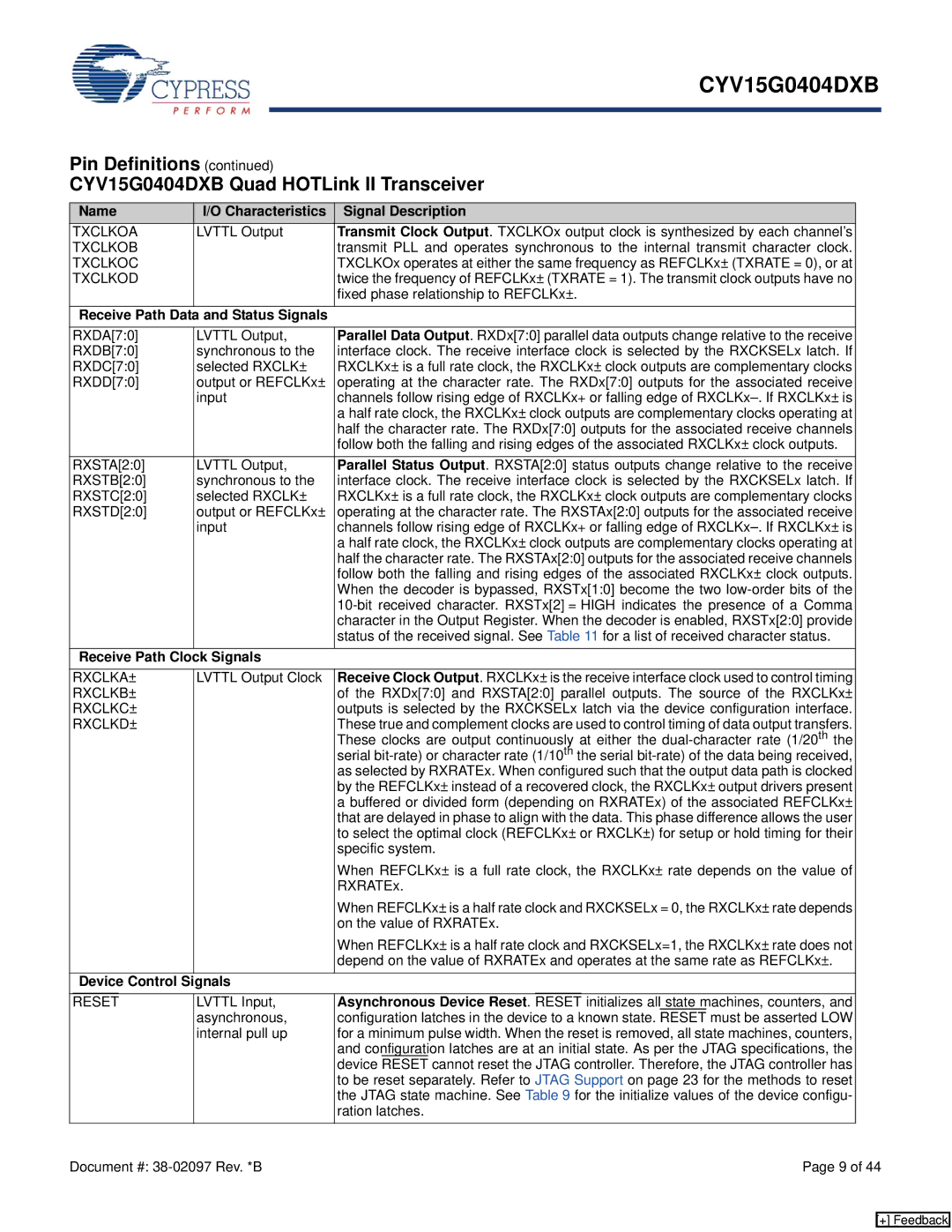
Name | I/O Characteristics | Signal Description |
| ||||
TXCLKOA | LVTTL Output | Transmit Clock Output. TXCLKOx output clock is synthesized by each channel’s |
| ||||
TXCLKOB |
| transmit PLL and operates synchronous to the internal transmit character clock. |
| ||||
TXCLKOC |
| TXCLKOx operates at either the same frequency as REFCLKx± (TXRATE = 0), or at |
| ||||
TXCLKOD |
| twice the frequency of REFCLKx± (TXRATE = 1). The transmit clock outputs have no |
| ||||
|
| fixed phase relationship to REFCLKx±. |
| ||||
Receive Path Data | and Status Signals |
|
|
|
|
|
|
RXDA[7:0] | LVTTL Output, | Parallel Data Output. RXDx[7:0] parallel data outputs change relative to the receive |
| ||||
RXDB[7:0] | synchronous to the | interface clock. The receive interface clock is selected by the RXCKSELx latch. If |
| ||||
RXDC[7:0] | selected RXCLK± | RXCLKx± is a full rate clock, the RXCLKx± clock outputs are complementary clocks |
| ||||
RXDD[7:0] | output or REFCLKx± | operating at the character rate. The RXDx[7:0] outputs for the associated receive |
| ||||
| input | channels follow rising edge of RXCLKx+ or falling edge of |
| ||||
|
| a half rate clock, the RXCLKx± clock outputs are complementary clocks operating at |
| ||||
|
| half the character rate. The RXDx[7:0] outputs for the associated receive channels |
| ||||
|
| follow both the falling and rising edges of the associated RXCLKx± clock outputs. |
| ||||
RXSTA[2:0] | LVTTL Output, | Parallel Status Output. RXSTA[2:0] status outputs change relative to the receive |
| ||||
RXSTB[2:0] | synchronous to the | interface clock. The receive interface clock is selected by the RXCKSELx latch. If |
| ||||
RXSTC[2:0] | selected RXCLK± | RXCLKx± is a full rate clock, the RXCLKx± clock outputs are complementary clocks |
| ||||
RXSTD[2:0] | output or REFCLKx± | operating at the character rate. The RXSTAx[2:0] outputs for the associated receive |
| ||||
| input | channels follow rising edge of RXCLKx+ or falling edge of |
| ||||
|
| a half rate clock, the RXCLKx± clock outputs are complementary clocks operating at |
| ||||
|
| half the character rate. The RXSTAx[2:0] outputs for the associated receive channels |
| ||||
|
| follow both the falling and rising edges of the associated RXCLKx± clock outputs. |
| ||||
|
| When the decoder is bypassed, RXSTx[1:0] become the two |
| ||||
|
|
| |||||
|
| character in the Output Register. When the decoder is enabled, RXSTx[2:0] provide |
| ||||
|
| status of the received signal. See Table 11 for a list of received character status. |
| ||||
Receive Path Clock Signals |
|
|
|
|
|
| |
RXCLKA± | LVTTL Output Clock | Receive Clock Output. RXCLKx± is the receive interface clock used to control timing |
| ||||
RXCLKB± |
| of the RXDx[7:0] and RXSTA[2:0] parallel outputs. The source of the RXCLKx± |
| ||||
RXCLKC± |
| outputs is selected by the RXCKSELx latch via the device configuration interface. |
| ||||
RXCLKD± |
| These true and complement clocks are used to control timing of data output transfers. |
| ||||
|
| These clocks are output continuously at either the |
| ||||
|
| serial |
| ||||
|
| as selected by RXRATEx. When configured such that the output data path is clocked |
| ||||
|
| by the REFCLKx± instead of a recovered clock, the RXCLKx± output drivers present |
| ||||
|
| a buffered or divided form (depending on RXRATEx) of the associated REFCLKx± |
| ||||
|
| that are delayed in phase to align with the data. This phase difference allows the user |
| ||||
|
| to select the optimal clock (REFCLKx± or RXCLK±) for setup or hold timing for their |
| ||||
|
| specific system. |
| ||||
|
| When REFCLKx± is a full rate clock, the RXCLKx± rate depends on the value of |
| ||||
|
| RXRATEx. |
| ||||
|
| When REFCLKx± is a half rate clock and RXCKSELx = 0, the RXCLKx± rate depends |
| ||||
|
| on the value of RXRATEx. |
| ||||
|
| When REFCLKx± is a half rate clock and RXCKSELx=1, the RXCLKx± rate does not |
| ||||
|
| depend on the value of RXRATEx and operates at the same rate as REFCLKx±. |
| ||||
Device Control | Signals |
|
|
|
|
|
|
RESET | LVTTL Input, | Asynchronous Device Reset. | RESET | initializes all state machines, counters, and |
| ||
| asynchronous, | configuration latches in the device to a known state. | RESET | must be asserted LOW |
| ||
| internal pull up | for a minimum pulse width. When the reset is removed, all state machines, counters, |
| ||||
|
| and configuration latches are at an initial state. As per the JTAG specifications, the |
| ||||
|
| device RESET cannot reset the JTAG controller. Therefore, the JTAG controller has |
| ||||
|
| to be reset separately. Refer to JTAG Support on page 23 for the methods to reset |
| ||||
|
| the JTAG state machine. See Table 9 for the initialize values of the device configu- |
| ||||
|
| ration latches. |
| ||||
Document #: |
|
|
|
| Page 9 of 44 | ||
[+] Feedback