CYV15G0404DXB
Pin Definitions
CYV15G0404DXB Quad HOTLink II Transceiver
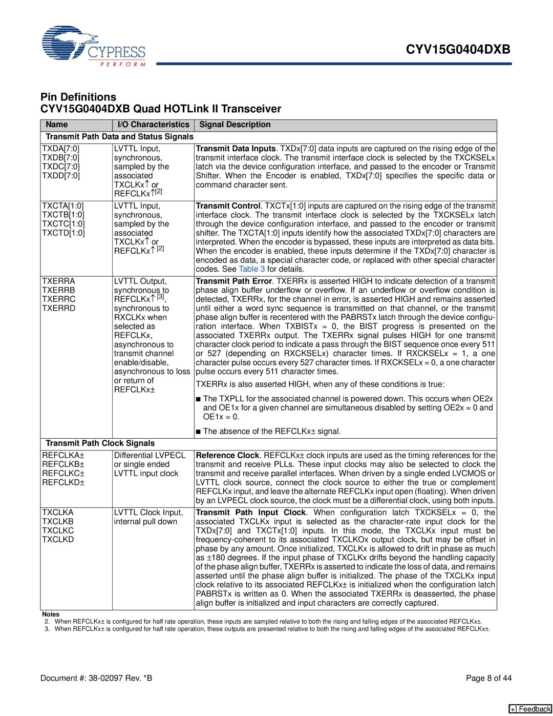
Name | I/O Characteristics | Signal Description |
Transmit Path Data and Status Signals |
| |
TXDA[7:0] | LVTTL Input, | Transmit Data Inputs. TXDx[7:0] data inputs are captured on the rising edge of the |
TXDB[7:0] | synchronous, | transmit interface clock. The transmit interface clock is selected by the TXCKSELx |
TXDC[7:0] | sampled by the | latch via the device configuration interface, and passed to the encoder or Transmit |
TXDD[7:0] | associated | Shifter. When the Encoder is enabled, TXDx[7:0] specifies the specific data or |
| TXCLKx↑ or | command character sent. |
| REFCLKx↑[2] |
|
TXCTA[1:0] | LVTTL Input, | Transmit Control. TXCTx[1:0] inputs are captured on the rising edge of the transmit |
TXCTB[1:0] | synchronous, | interface clock. The transmit interface clock is selected by the TXCKSELx latch |
TXCTC[1:0] | sampled by the | through the device configuration interface, and passed to the encoder or transmit |
TXCTD[1:0] | associated | shifter. The TXCTA[1:0] inputs identify how the associated TXDx[7:0] characters are |
| TXCLKx↑ or | interpreted. When the encoder is bypassed, these inputs are interpreted as data bits. |
| REFCLKx↑ [2] | When the encoder is enabled, these inputs determine if the TXDx[7:0] character is |
|
| encoded as data, a special character code, or replaced with other special character |
|
| codes. See Table 3 for details. |
TXERRA | LVTTL Output, | Transmit Path Error. TXERRx is asserted HIGH to indicate detection of a transmit |
TXERRB | synchronous to | phase align buffer underflow or overflow. If an underflow or overflow condition is |
TXERRC | REFCLKx↑ [3], | detected, TXERRx, for the channel in error, is asserted HIGH and remains asserted |
TXERRD | synchronous to | until either a word sync sequence is transmitted on that channel, or the transmit |
| RXCLKx when | phase align buffer is recentered with the PABRSTx latch through the device configu- |
| selected as | ration interface. When TXBISTx = 0, the BIST progress is presented on the |
| REFCLKx, | associated TXERRx output. The TXERRx signal pulses HIGH for one transmit |
| asynchronous to | character clock period to indicate a pass through the BIST sequence once every 511 |
| transmit channel | or 527 (depending on RXCKSELx) character times. If RXCKSELx = 1, a one |
| enable/disable, | character pulse occurs every 527 character times. If RXCKSELx = 0, a one character |
| asynchronous to loss | pulse occurs every 511 character times. |
| or return of | TXERRx is also asserted HIGH, when any of these conditions is true: |
| REFCLKx± | |
| ■ The TXPLL for the associated channel is powered down. This occurs when OE2x | |
|
| |
|
| and OE1x for a given channel are simultaneous disabled by setting OE2x = 0 and |
|
| OE1x = 0. |
|
| ■ The absence of the REFCLKx± signal. |
|
|
|
Transmit Path Clock Signals |
| |
REFCLKA± | Differential LVPECL | Reference Clock. REFCLKx± clock inputs are used as the timing references for the |
REFCLKB± | or single ended | transmit and receive PLLs. These input clocks may also be selected to clock the |
REFCLKC± | LVTTL input clock | transmit and receive parallel interfaces. When driven by a single ended LVCMOS or |
REFCLKD± |
| LVTTL clock source, connect the clock source to either the true or complement |
|
| REFCLKx input, and leave the alternate REFCLKx input open (floating). When driven |
|
| by an LVPECL clock source, the clock must be a differential clock, using both inputs. |
TXCLKA | LVTTL Clock Input, | Transmit Path Input Clock. When configuration latch TXCKSELx = 0, the |
TXCLKB | internal pull down | associated TXCLKx input is selected as the |
TXCLKC |
| TXDx[7:0] and TXCTx[1:0] inputs. In this mode, the TXCLKx input must be |
TXCLKD |
| |
|
| phase by any amount. Once initialized, TXCLKx is allowed to drift in phase as much |
|
| as ±180 degrees. If the input phase of TXCLKx drifts beyond the handling capacity |
|
| of the phase align buffer, TXERRx is asserted to indicate the loss of data, and remains |
|
| asserted until the phase align buffer is initialized. The phase of the TXCLKx input |
|
| clock relative to its associated REFCLKx± is initialized when the configuration latch |
|
| PABRSTx is written as 0. When the associated TXERRx is deasserted, the phase |
|
| align buffer is initialized and input characters are correctly captured. |
Notes |
|
|
2.When REFCLKx± is configured for half rate operation, these inputs are sampled relative to both the rising and falling edges of the associated REFCLKx±.
3.When REFCLKx± is configured for half rate operation, these outputs are presented relative to both the rising and falling edges of the associated REFCLKx±.
Document #: | Page 8 of 44 |
[+] Feedback