CYV15G0404DXB
Maximum Ratings
Exceeding maximum ratings may impair the useful life of device. These user guidelines are not tested.
Static Discharge Voltage | > 2000 V |
(according to |
|
> 200 mA |
Storage Temperature | ||
Ambient Temperature with |
|
|
Power Applied | ||
Supply Voltage to Ground Potential | ||
DC Voltage Applied to LVTTL Outputs |
|
|
in | ||
Output Current into LVTTL Outputs (LOW) | ................. 60 mA | |
DC Input Voltage | ||
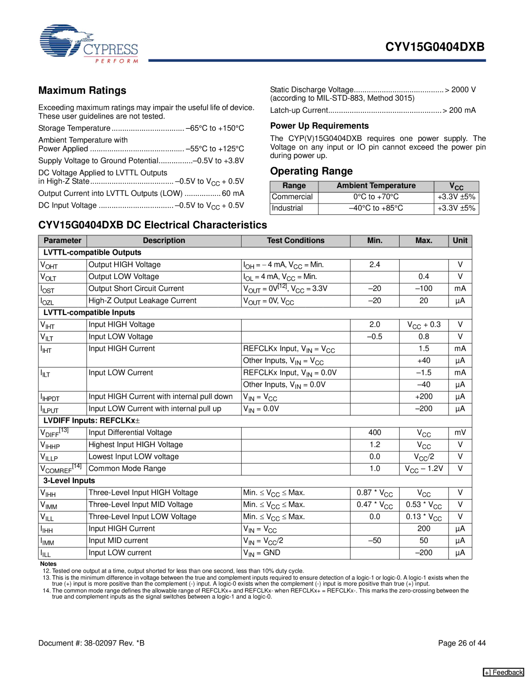
CYV15G0404DXB DC Electrical Characteristics
Power Up Requirements
The CYP(V)15G0404DXB requires one power supply. The Voltage on any input or IO pin cannot exceed the power pin during power up.
Operating Range
Range | Ambient Temperature | VCC |
Commercial | 0°C to +70°C | +3.3V ±5% |
Industrial | +3.3V ±5% |
Parameter | Description | Test Conditions | Min. | Max. | Unit |
|
|
|
| ||
|
|
|
|
|
|
VOHT | Output HIGH Voltage | IOH = − 4 mA, VCC = Min. | 2.4 |
| V |
VOLT | Output LOW Voltage | IOL = 4 mA, VCC = Min. |
| 0.4 | V |
IOST | Output Short Circuit Current | VOUT = 0V[12], VCC = 3.3V | mA | ||
IOZL | VOUT = 0V, VCC | 20 | µA | ||
|
|
|
|
| |
VIHT | Input HIGH Voltage |
| 2.0 | VCC + 0.3 | V |
VILT | Input LOW Voltage |
| 0.8 | V | |
IIHT | Input HIGH Current | REFCLKx Input, VIN = VCC |
| 1.5 | mA |
|
| Other Inputs, VIN = VCC |
| +40 | µA |
IILT | Input LOW Current | REFCLKx Input, VIN = 0.0V |
| mA | |
|
| Other Inputs, VIN = 0.0V |
| µA | |
IIHPDT | Input HIGH Current with internal pull down | VIN = VCC |
| +200 | µA |
IILPUT | Input LOW Current with internal pull up | VIN = 0.0V |
| µA | |
LVDIFF Inputs: REFCLKx± |
|
|
|
| |
VDIFF[13] | Input Differential Voltage |
| 400 | VCC | mV |
VIHHP | Highest Input HIGH Voltage |
| 1.2 | VCC | V |
VILLP | Lowest Input LOW voltage |
| 0.0 | VCC/2 | V |
VCOMREF[14] | Common Mode Range |
| 1.0 | VCC – 1.2V | V |
|
|
|
|
| |
|
|
|
|
|
|
VIHH | Min. ≤ VCC ≤ Max. | 0.87 * VCC | VCC | V | |
VIMM | Min. ≤ VCC ≤ Max. | 0.47 * VCC | 0.53 * VCC | V | |
VILL | Min. ≤ VCC ≤ Max. | 0.0 | 0.13 * VCC | V | |
IIHH | Input HIGH Current | VIN = VCC |
| 200 | µA |
IIMM | Input MID current | VIN = VCC/2 | 50 | µA | |
IILL | Input LOW current | VIN = GND |
| µA | |
Notes
12.Tested one output at a time, output shorted for less than one second, less than 10% duty cycle.
13.This is the minimum difference in voltage between the true and complement inputs required to ensure detection of a
14.The common mode range defines the allowable range of REFCLKx+ and REFCLKx- when REFCLKx+ =
Document #: | Page 26 of 44 |
[+] Feedback
