CYV15G0404DXB
Pin Definitions (continued)
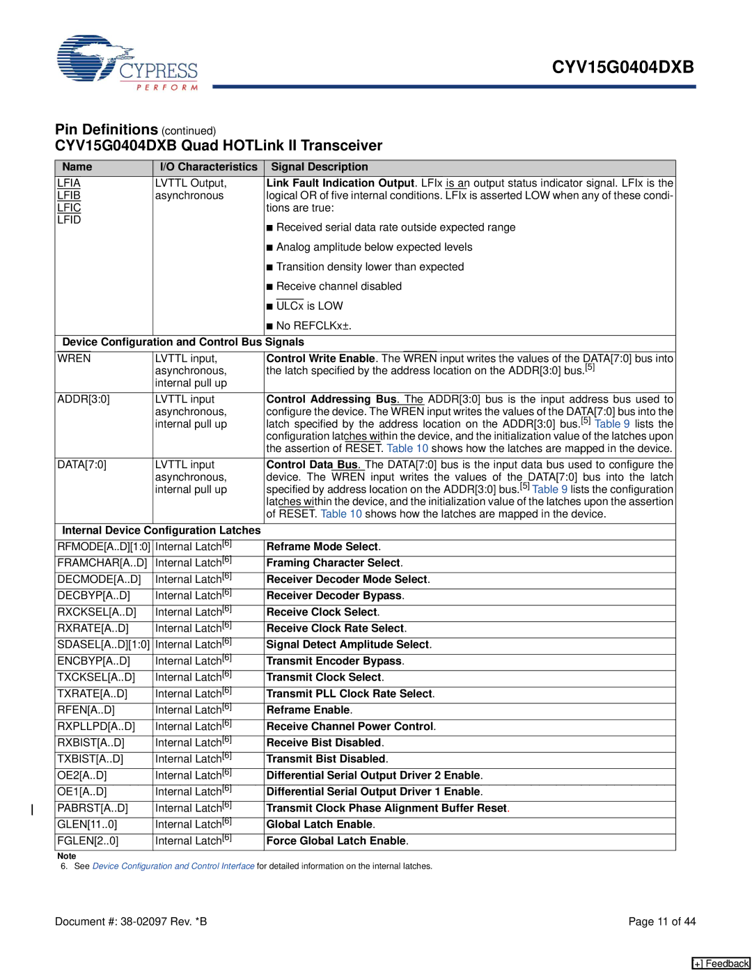
CYV15G0404DXB Quad HOTLink II Transceiver
Name | I/O Characteristics | Signal Description | ||||||||||
LFIA | LVTTL Output, | Link Fault Indication Output. | LFIx | is an output status indicator signal. | LFIx | is the | ||||||
LFIB | asynchronous | logical OR of five internal conditions. LFIx is asserted LOW when any of these condi- | ||||||||||
LFIC |
| tions are true: | ||||||||||
LFID |
| ■ Received serial data rate outside expected range | ||||||||||
|
| |||||||||||
|
| ■ Analog amplitude below expected levels | ||||||||||
|
| ■ Transition density lower than expected | ||||||||||
|
| ■ Receive channel disabled | ||||||||||
|
| ■ |
| is LOW | ||||||||
|
| ULCx | ||||||||||
|
| ■ No REFCLKx±. | ||||||||||
|
|
| ||||||||||
Device Configuration and Control Bus Signals | ||||||||||||
WREN | LVTTL input, | Control Write Enable. The | WREN | input writes the values of the DATA[7:0] bus into | ||||||||
| asynchronous, | the latch specified by the address location on the ADDR[3:0] bus.[5] | ||||||||||
| internal pull up |
|
|
|
|
|
|
|
|
|
|
|
ADDR[3:0] | LVTTL input | Control Addressing Bus. The ADDR[3:0] bus is the input address bus used to | ||||||||||
| asynchronous, | configure the device. The WREN input writes the values of the DATA[7:0] bus into the | ||||||||||
| internal pull up | latch specified by the address location on the ADDR[3:0] bus.[5] Table 9 lists the | ||||||||||
|
| configuration latches within the device, and the initialization value of the latches upon | ||||||||||
|
| the assertion of RESET. Table 10 shows how the latches are mapped in the device. | ||||||||||
DATA[7:0] | LVTTL input | Control Data Bus. The DATA[7:0] bus is the input data bus used to configure the | ||||||||||
| asynchronous, | device. The | WREN | input writes the values of the DATA[7:0] bus into the latch | ||||||||
| internal pull up | specified by address location on the ADDR[3:0] bus.[5] Table 9 lists the configuration | ||||||||||
|
| latches within the device, and the initialization value of the latches upon the assertion | ||||||||||
|
| of RESET. Table 10 shows how the latches are mapped in the device. | ||||||||||
Internal Device | Configuration Latches |
|
|
|
|
|
|
|
|
|
|
|
RFMODE[A..D][1:0] | Internal Latch[6] | Reframe Mode Select. | ||||||||||
FRAMCHAR[A..D] | Internal Latch[6] | Framing Character Select. | ||||||||||
DECMODE[A..D] | Internal Latch[6] | Receiver Decoder Mode Select. | ||||||||||
DECBYP[A..D] | Internal Latch[6] | Receiver Decoder Bypass. | ||||||||||
RXCKSEL[A..D] | Internal Latch[6] | Receive Clock Select. | ||||||||||
RXRATE[A..D] | Internal Latch[6] | Receive Clock Rate Select. | ||||||||||
SDASEL[A..D][1:0] | Internal Latch[6] | Signal Detect Amplitude Select. | ||||||||||
ENCBYP[A..D] | Internal Latch[6] | Transmit Encoder Bypass. | ||||||||||
TXCKSEL[A..D] | Internal Latch[6] | Transmit Clock Select. | ||||||||||
TXRATE[A..D] | Internal Latch[6] | Transmit PLL Clock Rate Select. | ||||||||||
RFEN[A..D] | Internal Latch[6] | Reframe Enable. | ||||||||||
RXPLLPD[A..D] | Internal Latch[6] | Receive Channel Power Control. | ||||||||||
RXBIST[A..D] | Internal Latch[6] | Receive Bist Disabled. | ||||||||||
TXBIST[A..D] | Internal Latch[6] | Transmit Bist Disabled. | ||||||||||
OE2[A..D] | Internal Latch[6] | Differential Serial Output Driver 2 Enable. | ||||||||||
OE1[A..D] | Internal Latch[6] | Differential Serial Output Driver 1 Enable. | ||||||||||
PABRST[A..D] | Internal Latch[6] | Transmit Clock Phase Alignment Buffer Reset. | ||||||||||
GLEN[11..0] | Internal Latch[6] | Global Latch Enable. | ||||||||||
FGLEN[2..0] | Internal Latch[6] | Force Global Latch Enable. | ||||||||||
Note
6. See Device Configuration and Control Interface for detailed information on the internal latches.
Document #: | Page 11 of 44 |
[+] Feedback