It is very easy to do
3.4.1 DA1
The op amp supporting DA1 converts
R28 is present solely to balance the op amp input current bias. R25 helps to achieve a volt- age close to ground for a 0% duty cycle.
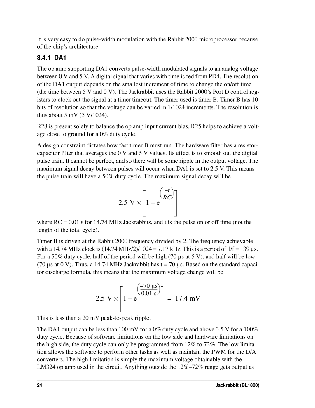
A design constraint dictates how fast timer B must run. The hardware filter has a resistor- capacitor filter that averages the 0 V and 5 V values. Its effect is to smooth out the digital pulse train. It cannot be perfect, and so there will be some ripple in the output voltage. The maximum signal decay between pulses will occur when DA1 is set to 2.5 V. This means the pulse train will have a 50% duty cycle. The maximum signal decay will be
⎛
2.5 V ⋅ 1 – e RC
where RC = 0.01 s for 14.74 MHz Jackrabbits, and t is the pulse on or off time (not the length of the total cycle).
Timer B is driven at the Rabbit 2000 frequency divided by 2. The frequency achievable with a 14.74 MHz clock is (14.74 MHz/2)/1024 = 7.17 kHz. This is a period of 1/f = 139 µs. For a 50% duty cycle, half of the period will be high (70 µs at 5 V), and half will be low (70 µs at 0 V). Thus, a 14.74 MHz Jackrabbit has t = 70 µs. Based on the standard capaci- tor discharge formula, this means that the maximum voltage change will be
|
| ⎛ |
|
| |
2.5 V ⋅ |
| ⎝ 0.01 s ⎠ |
| 1 – e | |
|
|
|
= 17.4 mV
This is less than a 20 mV
The DA1 output can be less than 100 mV for a 0% duty cycle and above 3.5 V for a 100% duty cycle. Because of software limitations on the low side and hardware limitations on the high side, the duty cycle can only be programmed from 12% to 72%. The low limita- tion allows the software to perform other tasks as well as maintain the PWM for the D/A converters. The high limitation is simply the maximum voltage obtainable with the LM324 op amp used in the circuit. Anything outside the
24 | Jackrabbit (BL1800) |