4.4 Jackrabbit Function Calls
4.4.1 I/O Drivers
The Jackrabbit contains four
4.4.1.1 Initialization
The function jrioInit() must be called before any other function from the JRIO.LIB library. This function initializes the digital outputs and sets up the driver for the analog input/outputs. The digital outputs correspond to the Rabbit processor’s port E bits
The function void jrioInit() initializes the I/O drivers for Jackrabbit. In particular, it sets up parallel port D bits 1, 2, and 4 for analog output, port E bits
4.4.1.2 Digital Outputs
The Jackrabbit contains four
HV0, HV1, and HV2 are
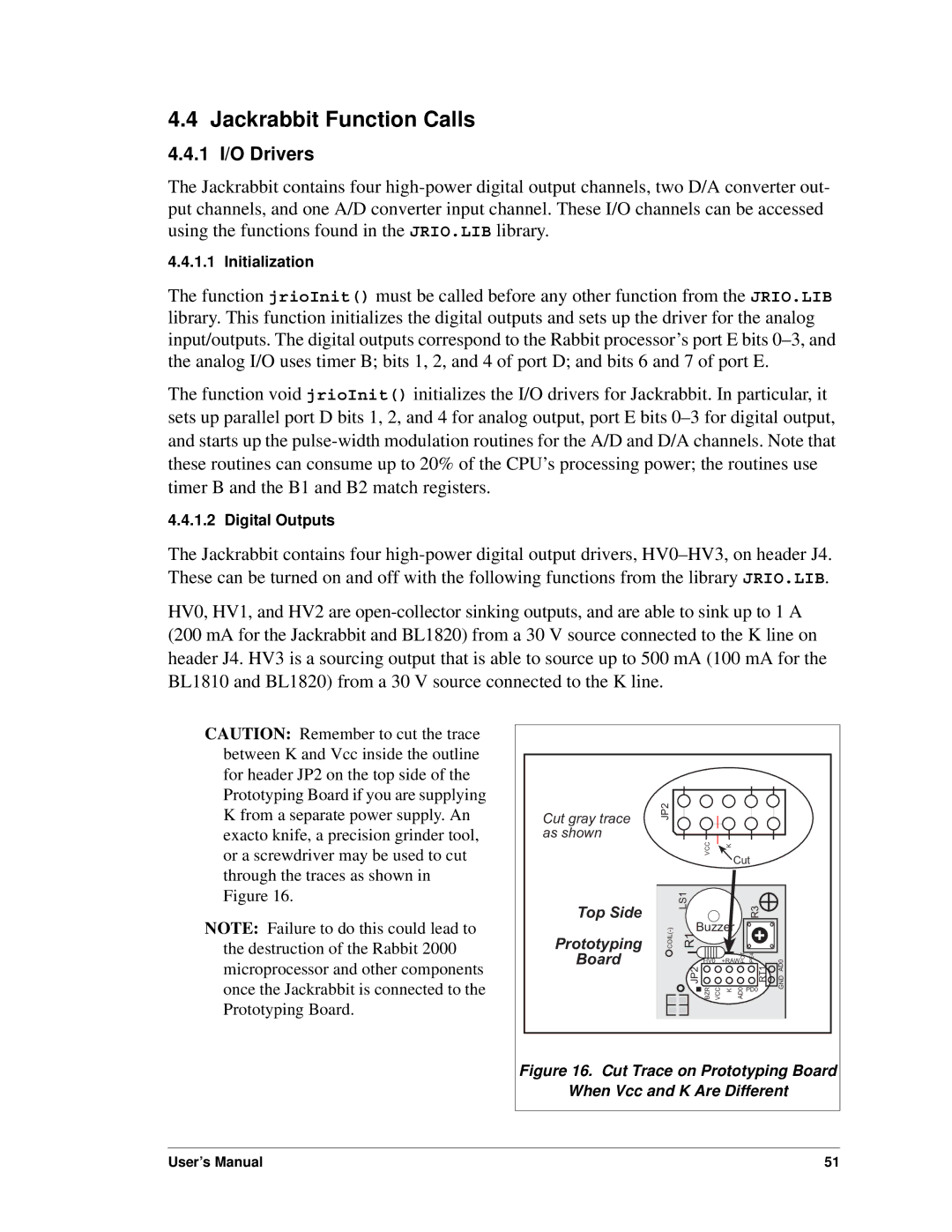
CAUTION: Remember to cut the trace between K and Vcc inside the outline for header JP2 on the top side of the Prototyping Board if you are supplying K from a separate power supply. An exacto knife, a precision grinder tool, or a screwdriver may be used to cut through the traces as shown in Figure 16.
NOTE: Failure to do this could lead to
the destruction of the Rabbit 2000 microprocessor and other components once the Jackrabbit is connected to the Prototyping Board.
Cut gray trace as shown
Top Side
Prototyping
Board
JP2 |
|
|
|
|
|
|
|
| VCC | K |
|
|
|
|
|
| Cut |
| ||
| LS1 |
|
|
| R3 |
|
| Buzzer |
| 3 |
| ||
|
| 2 |
| |||
|
|
|
|
|
| |
COIL()- | R1 |
|
|
| + |
|
|
|
| 1 |
| ||
|
| HV0 | +RAWPOT PE4 | GND AD0 | ||
| JP2 |
|
|
| RT1 | |
| BZR VCC | K | AD0 | PD0 | ||
|
| |||||
Figure 16. Cut Trace on Prototyping Board
When Vcc and K Are Different
User’s Manual | 51 |