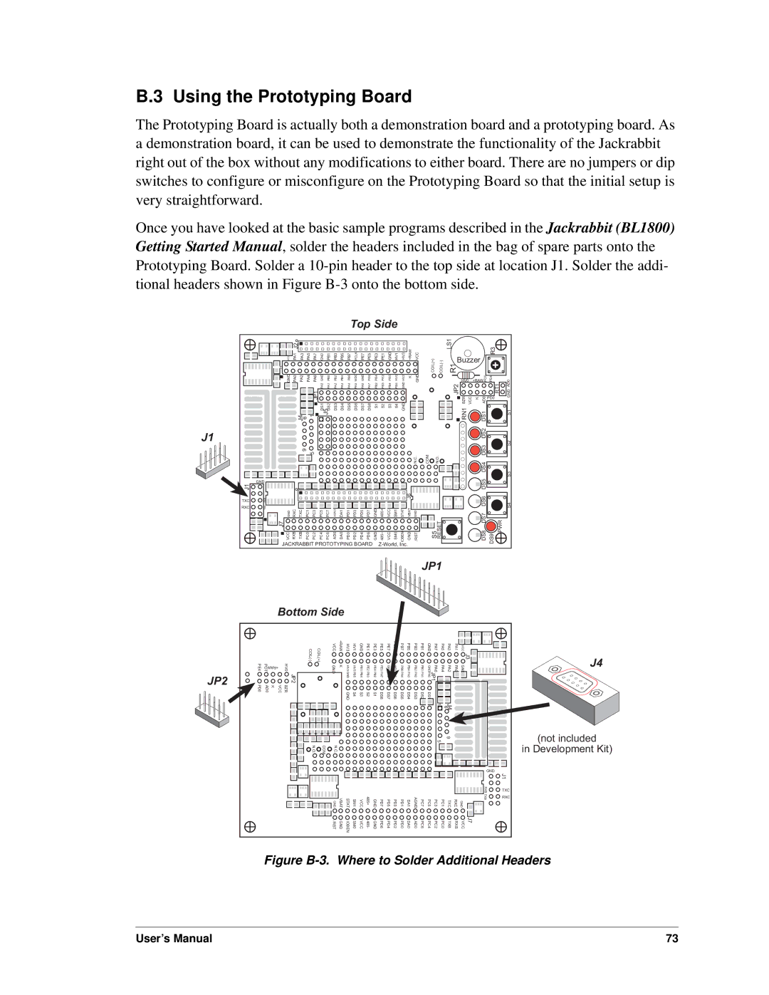
B.3 Using the Prototyping Board
The Prototyping Board is actually both a demonstration board and a prototyping board. As a demonstration board, it can be used to demonstrate the functionality of the Jackrabbit right out of the box without any modifications to either board. There are no jumpers or dip switches to configure or misconfigure on the Prototyping Board so that the initial setup is very straightforward.
Once you have looked at the basic sample programs described in the Jackrabbit (BL1800) Getting Started Manual, solder the headers included in the bag of spare parts onto the Prototyping Board. Solder a
J1
|
|
|
|
|
|
|
|
|
|
|
|
| Top Side |
|
|
|
|
|
|
|
|
|
|
| |||||||
|
|
|
| J2 | PA3 | PA5 | PA7 | GND | PB1 | PB3 | PB5 | PB7 | PCLK | PE7 | PE5 | PE3 | PE1 | GND | HV1 | HV3 | +RAW | VCC | COIL(+) | LS1 |
|
| R3 |
|
| ||
|
| J3 | VCC | PA1 | R1 |
|
|
| 1 |
| |||||||||||||||||||||
|
|
|
|
|
|
|
|
|
|
|
|
|
|
|
|
|
|
|
|
|
|
|
|
|
| Buzzer |
|
| 3 |
| |
|
|
|
|
|
|
|
|
|
|
|
|
|
|
|
|
|
|
|
|
|
|
|
|
|
|
|
|
| + |
| |
|
|
|
| PA0 J4 |
|
|
|
|
| DS3PA2 PB2 | DS4PA3 PB4 | DS5PA4 PB6 | DS6PA5 WDO | DS7PA6 GND | DS8PA7 PE6 | S1 PB2 PE4 | S2 PB3 PE2 | S3 PB4 PE0 | S4 PB5 HV0 | GNDGND HV2 |
|
|
|
| JP2 RN1BZR VCC |
| DS1AD0 | 2 | GNDS1 AD0 | ||
|
|
| GND |
| 1 | J5 | K | GND |
|
| K |
|
| ||||||||||||||||||
|
|
|
|
| PA2 | PA4 | PA6 | GND | PB0 |
|
|
|
|
|
|
|
|
|
|
|
|
|
|
| HV0 | +RAWPOT PE4 |
|
| |||
|
|
|
|
|
|
|
| JP1 | PA0 | PA1 |
|
|
|
|
|
|
|
|
|
|
|
|
|
|
|
|
|
| RT1 |
| |
|
|
|
|
|
|
|
|
|
|
|
|
|
|
|
|
|
|
|
|
|
|
|
|
|
|
|
| PD0 |
|
| |
|
|
|
|
|
|
|
|
| DS1 | DS2 |
|
|
|
|
|
|
|
|
|
|
|
|
|
|
|
|
|
|
|
|
|
|
|
|
|
| 6 |
|
|
|
|
|
|
|
|
|
|
|
|
|
|
|
|
|
|
|
|
|
|
|
|
| |
|
|
|
|
|
|
|
|
|
|
|
|
|
|
|
|
|
|
|
|
|
|
|
|
|
|
|
| DS2 |
|
|
|
|
|
|
|
| 9 | 5 |
|
|
|
|
|
|
|
|
|
|
|
|
|
| N.C. | COM | N.O. |
|
| DS4 DS3 |
|
| S3S2 | ||
| GND |
|
|
|
|
|
|
|
|
|
|
|
|
|
|
|
|
|
|
|
|
|
|
|
|
|
| DS5 |
|
|
|
TXC | TXBRXB | J7 | VCC | RXCRXB | TXCTXB | PC1PC0 | PC3PC2 | PC5PC4 | PC7PC6 | AD0AGND | DA1DA0 | PD1PD0 | PD3PD2 | PD5PD4 | PD7PD6 | GNDGND | 485+485– | VCCVCC | SM1SM0 | IOBENSTAT | GNDVBATJ6 | /RSTGND |
| RESET |
|
| DS6DS7DS8 | DS9 | PWR | S4 | |
RXC |
|
|
|
|
|
|
|
|
|
|
|
|
|
|
|
|
|
|
|
|
|
|
|
|
|
|
|
|
|
|
|
|
|
| GND |
|
|
|
|
|
|
|
|
|
|
|
|
|
|
|
|
|
|
|
|
|
|
|
|
|
|
|
|
|
|
|
|
|
|
|
|
|
|
|
|
|
|
|
|
|
|
|
|
|
|
|
| S5 |
|
|
|
|
|
| |
|
| JACKRABBIT PROTOTYPING BOARD |
|
|
|
|
|
|
|
|
|
| |||||||||||||||||||
JP1
Bottom Side
|
|
|
|
| COIL(+) | VCC | +RAW | HV3 | HV1 | GND | PE1 | PE3 | PE5 | PE7 | PCLK | PB7 | PB5 | PB3 | PB1 | GND | PA7 | PA5 | PA3 | PA1 | VCC | J3 |
| |
PE4 | +RAW |
| HV0 |
|
|
|
|
|
|
|
|
|
|
|
|
|
|
|
|
| PA6 |
|
|
|
|
|
| |
POT |
|
| JP2 |
| GND | K | HV2GND | HV0PB5 | PE0PB4 | PE2PB3 | PE4PB2 | PE6PA7 |
|
| PB6PA4 | PB4PA3 | PB2PA2 | PB0PA1 |
| PA4 | PA2 | PA0 | GND |
|
| |||
|
|
|
|
| JP1 GNDPA0 |
|
| |||||||||||||||||||||
JP2 |
|
|
|
|
|
|
|
|
|
|
|
|
|
|
|
|
|
|
|
|
|
|
|
|
|
|
|
|
PD0 | AD0 | K | VCC | BZR |
|
|
|
| GND | S4 | S3 | S2 | S1 | DS8 | DS7 | DS6 | DS5 | DS4 | DS3 | DS2 | DS1 |
|
|
|
|
|
|
|
|
|
|
|
|
|
|
|
|
|
|
|
|
|
|
|
|
|
|
|
|
|
| 6 |
|
|
|
| |
|
|
|
|
|
|
|
|
|
|
|
|
|
|
|
|
|
|
|
|
|
| 1 | J4 |
|
|
|
| |
|
|
|
|
|
|
|
|
|
|
|
|
|
|
|
|
|
|
|
|
|
|
|
| 9 |
|
|
|
|
|
|
|
|
|
|
|
|
|
|
|
|
|
|
|
|
|
|
|
|
|
| 5 |
|
|
|
|
| |
|
|
|
|
| N.O. | COM | N.C. |
|
|
|
|
|
|
|
|
|
|
|
|
|
|
|
|
|
|
|
|
|
|
|
|
|
|
|
|
|
|
|
|
|
|
|
|
|
|
|
|
|
|
|
|
|
|
|
| GND | J1 |
|
|
|
|
|
|
|
|
|
|
|
|
|
|
|
|
|
|
|
|
|
|
|
|
|
|
|
| |
|
|
|
|
|
|
|
|
|
|
|
|
|
|
|
|
|
|
|
|
|
|
|
|
|
|
| RXB | TXC |
|
|
|
|
|
|
|
| VBAT | STAT | SM1 | VCC | 485+ | GND | PD7 | PD5 | PD3 | PD1 | DA1 | AGND | PC7 | PC5 | PC3 | PC1 | TXC | RXC |
| TXB | RXC |
|
|
|
|
|
|
| GND | GND |
| |||||||||||||||||||
|
|
|
|
|
|
| /RST | GND | IOBEN | SM0 | VCC | 485- | GND | PD6 | PD4 | PD2 | PD0 | DA0 | AD0 | PC6 | PC4 | PC2 | PC0 | TXB | RXB | VCC | J7 |
|
J4
(not included
in Development Kit)
Figure B-3. Where to Solder Additional Headers
User’s Manual | 73 |