C.2.1 Battery Backup Circuit
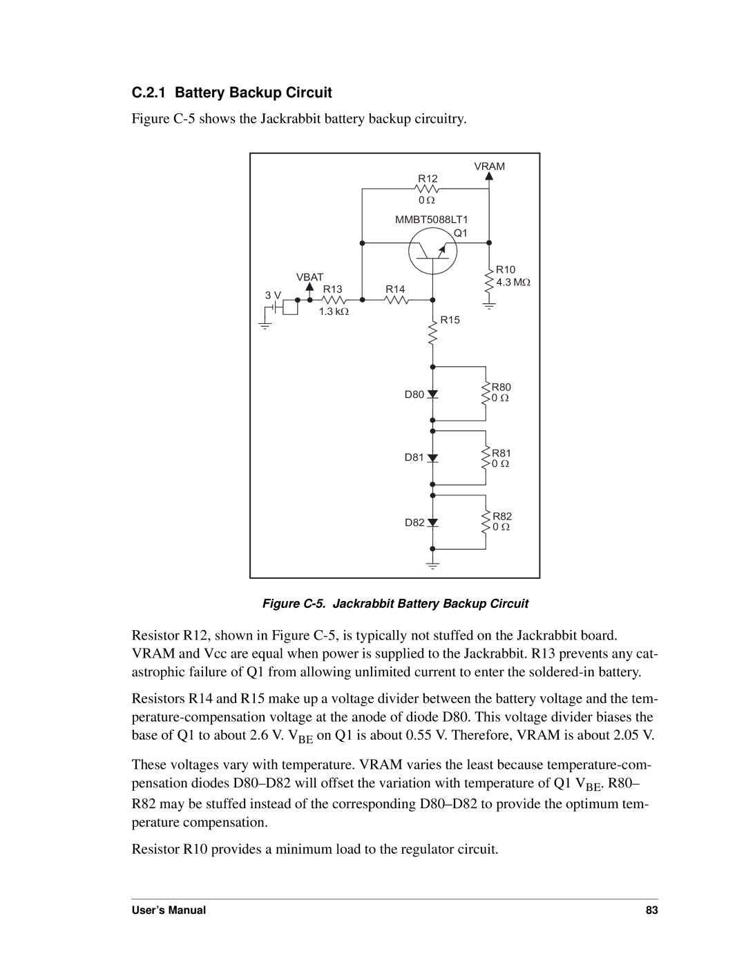
Figure C-5 shows the Jackrabbit battery backup circuitry.
|
| R12 | VRAM |
|
|
| |
|
| 0 W |
|
|
| MMBT5088LT1 |
|
|
| Q1 |
|
| VBAT |
| R10 |
|
| 4.3 MW | |
| R13 | R14 | |
3 V |
| ||
|
|
| |
| 1.3 kW | R15 |
|
|
|
| |
|
| D80 | R80 |
|
| 0 W | |
|
|
| |
|
| D81 | R81 |
|
| 0 W | |
|
|
| |
|
| D82 | R82 |
|
| 0 W | |
|
|
|
Figure C-5. Jackrabbit Battery Backup Circuit
Resistor R12, shown in Figure
Resistors R14 and R15 make up a voltage divider between the battery voltage and the tem-
These voltages vary with temperature. VRAM varies the least because
R82 may be stuffed instead of the corresponding
Resistor R10 provides a minimum load to the regulator circuit.
User’s Manual | 83 |