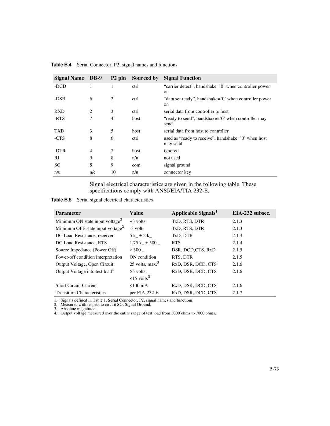
Table B.4 Serial Connector, P2, signal names and functions
Signal Name |
| P2 pin | Sourced by | Signal Function |
|
|
|
|
|
1 | 1 | ctrl | “carrier detect”, handshake=’0’ when controller power | |
|
|
|
| on |
6 | 2 | ctrl | “data set ready”, handshake=’0’ when controller power | |
|
|
|
| on |
RXD | 2 | 3 | ctrl | serial data from controller to host |
7 | 4 | host | “ready to send”, handshake=’0’ when controller may | |
|
|
|
| send |
TXD | 3 | 5 | host | serial data from host to controller |
8 | 6 | ctrl | used as “ready to receive”, handshake=’0’ when host | |
|
|
|
| may send |
4 | 7 | host | ignored | |
RI | 9 | 8 | n/u | not used |
SG | 5 | 9 | com | signal ground |
n/u | n/c | 10 | n/u | connector key |
|
|
|
|
|
Signal electrical characteristics are given in the following table. These specifications comply with ANSI/EIA/TIA
Table B.5 Serial signal electrical characteristics
Parameter | Value | Applicable Signals1 |
|
Minimum ON state input voltage2 | +3 volts | TxD, RTS, DTR | 2.1.3 |
Minimum OFF state input voltage2 | TxD, RTS, DTR | 2.1.3 | |
DC Load Resistance, receiver | 5 k_ ± 2 k_ | TxD, DTR | 2.1.4 |
DC Load Resistance, RTS | 1.75 k_ ± 500 _ | RTS | 2.1.4 |
Source Impedance (Power Off) | > 300 _ | DSR, DCD,CTS, RxD | 2.1.5 |
ON condition | RTS, DTR | 2.1.5 | |
Output Voltage, Open Circuit | 25 volts, max.3 | RxD, DSR, DCD, CTS | 2.1.6 |
Output Voltage into test load4 | >5 volts; | RxD, DSR, DCD, CTS | 2.1.6 |
| <15 volts3 |
|
|
Short Circuit Current | <100 mA | RxD, DSR, DCD, CTS | 2.1.6 |
Transition Characteristics | per | RxD, DSR, DCD, CTS | 2.1.7 |
1.Signals defined in Table 1. Serial Connector, P2, signal names and functions
2.Measured with respect to circuit SG, Signal Ground.
3.Absolute magnitude.
4.Output voltage measured over the entire range of test load from 3000 ohms to 7000 ohms.
