Introduction
2.5JTAG
•Compliant with IEEE Standard Test Access Port and Boundary Scan Architecture 1149.1a
2.6Related Documents
•Intel® 41210 Serial to Parallel PCI Bridge Design Specification (EDS), Revision 1.0.
•PCI Express Specification, Revision 1.0, from
•PCI Express Design Guide, Revision 0.5
•PCI Local Bus Specification, Revision 2.3, from
•
•IEEE Standard Test Access Port and Boundary Scan Architecture 1149.1a
•System Management Bus Specification, Revision 2.0
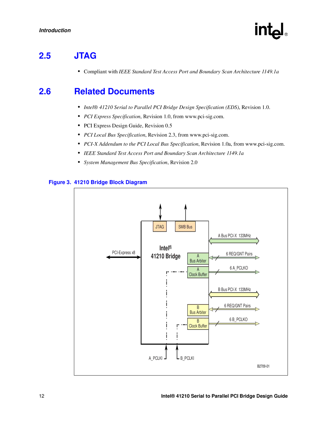
Figure 3. 41210 Bridge Block Diagram
|
|
|
|
|
|
|
|
|
|
|
|
|
|
| JTAG |
| SMB Bus |
| ||
|
|
|
|
|
|
|
Intelfi
41210 Bridge A
Bus Arbiter
A
Clock Buffer
B
Bus Arbiter
B
Clock Buffer
A_PCLKI |
|
|
| B_PCLKI |
|
|
A Bus
6 REQ/GNT Pairs
6 A_PCLKO
B Bus
6 REQ/GNT Pairs
6 B_PCLKO
12 | Intel® 41210 Serial to Parallel PCI Bridge Design Guide |