PCI-X Layout Guidelines
8.6.2Embedded PCI-X 100 MHz
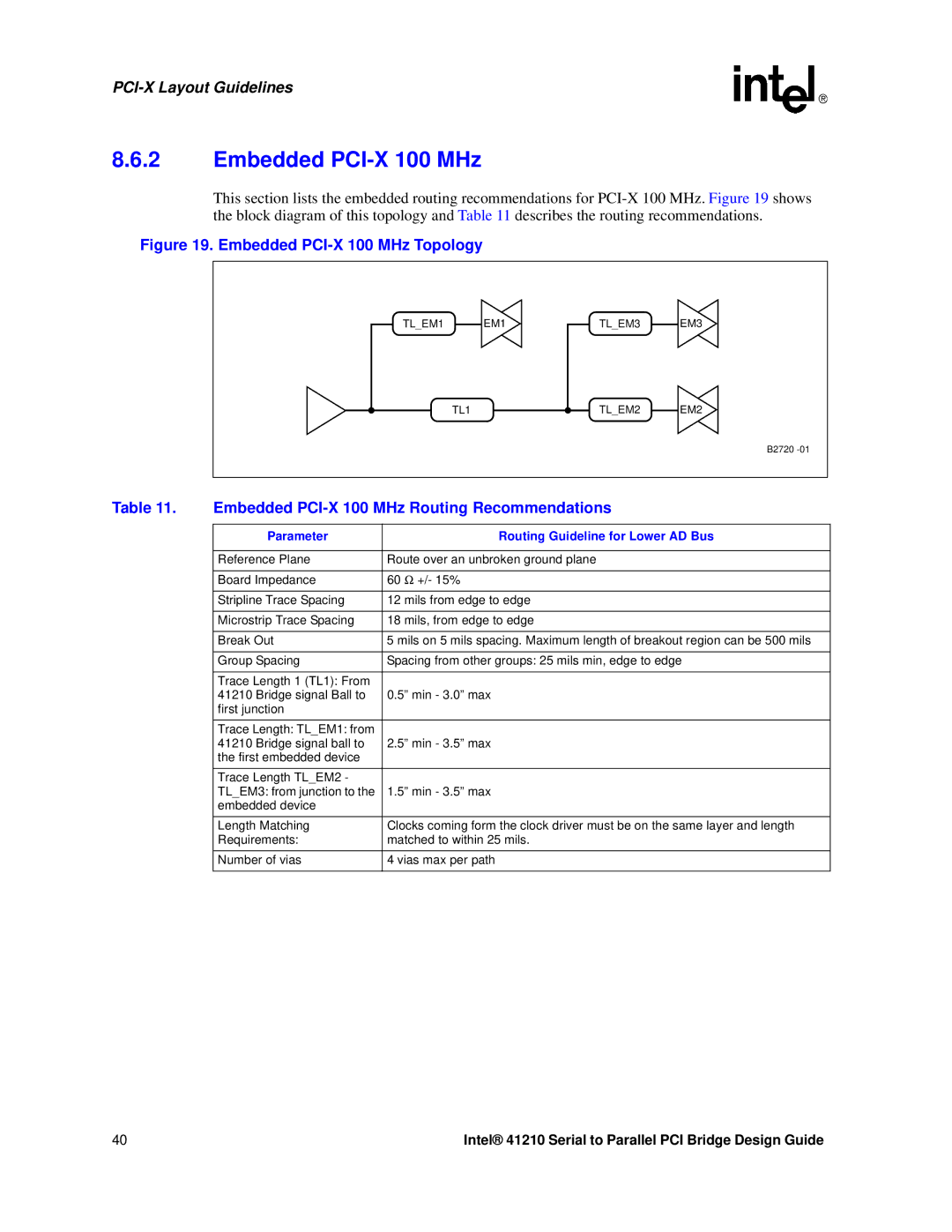
This section lists the embedded routing recommendations for
Figure 19. Embedded PCI-X 100 MHz Topology
TL_EM1 EM1
TL1
TL_EM3 EM3
TL_EM2 EM2
B2720
Table 11. | Embedded | |
|
|
|
| Parameter | Routing Guideline for Lower AD Bus |
|
|
|
| Reference Plane | Route over an unbroken ground plane |
|
|
|
| Board Impedance | 60 Ω +/- 15% |
|
|
|
| Stripline Trace Spacing | 12 mils from edge to edge |
|
|
|
| Microstrip Trace Spacing | 18 mils, from edge to edge |
|
|
|
| Break Out | 5 mils on 5 mils spacing. Maximum length of breakout region can be 500 mils |
|
|
|
| Group Spacing | Spacing from other groups: 25 mils min, edge to edge |
|
|
|
| Trace Length 1 (TL1): From |
|
| 41210 Bridge signal Ball to | 0.5” min - 3.0” max |
| first junction |
|
|
|
|
| Trace Length: TL_EM1: from |
|
| 41210 Bridge signal ball to | 2.5” min - 3.5” max |
| the first embedded device |
|
| Trace Length TL_EM2 - |
|
| TL_EM3: from junction to the | 1.5” min - 3.5” max |
| embedded device |
|
|
|
|
| Length Matching | Clocks coming form the clock driver must be on the same layer and length |
| Requirements: | matched to within 25 mils. |
|
|
|
| Number of vias | 4 vias max per path |
|
|
|
40 | Intel® 41210 Serial to Parallel PCI Bridge Design Guide |