Board Layout Guidelines
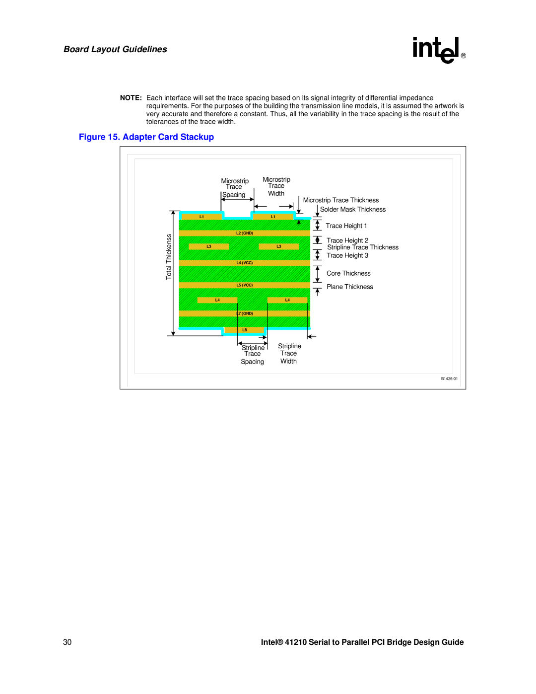
NOTE: Each interface will set the trace spacing based on its signal integrity of differential impedance requirements. For the purposes of the building the transmission line models, it is assumed the artwork is very accurate and therefore a constant. Thus, all the variability in the trace spacing is the result of the tolerances of the trace width.
Figure 15. Adapter Card Stackup
Total Thickenss
Microstrip
Trace
Spacing
L1
L2 (GND)
L3
L4 (VCC)
Microstrip
Trace
Width
L1
L3
Microstrip Trace Thickness Solder Mask Thickness
Trace Height 1
Trace Height 2
Stripline Trace Thickness
Trace Height 3
Core Thickness
L5 (VCC)
L4
L7 (GND)
L8
Stripline
Trace
Spacing
Plane Thickness
L4
Stripline
Trace
Width
30 | Intel® 41210 Serial to Parallel PCI Bridge Design Guide |