PCI-X Layout Guidelines
•Priority group for a master (i.e., whether a master is in low priority group or high priority group).
•Bus parking on last PCI agent or the bridge.
By default the arbiter parks the bus on the bridge and drives the A/D, C/BE# and PAR lines to a known value while the bus is idle.
8.2.1PCI Resistor Compensation
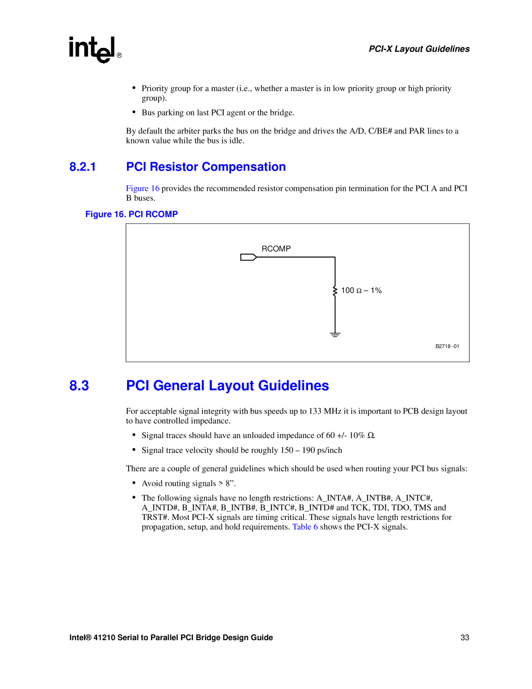
Figure 16 provides the recommended resistor compensation pin termination for the PCI A and PCI B buses.
Figure 16. PCI RCOMP
RCOMP
100 Ω – 1%
B2718
8.3PCI General Layout Guidelines
For acceptable signal integrity with bus speeds up to 133 MHz it is important to PCB design layout to have controlled impedance.
•Signal traces should have an unloaded impedance of 60 +/- 10% Ω .
•Signal trace velocity should be roughly 150 – 190 ps/inch
There are a couple of general guidelines which should be used when routing your PCI bus signals:
•Avoid routing signals > 8”.
•The following signals have no length restrictions: A_INTA#, A_INTB#, A_INTC#,
A_INTD#, B_INTA#, B_INTB#, B_INTC#, B_INTD# and TCK, TDI, TDO, TMS and TRST#. Most
Intel® 41210 Serial to Parallel PCI Bridge Design Guide | 33 |