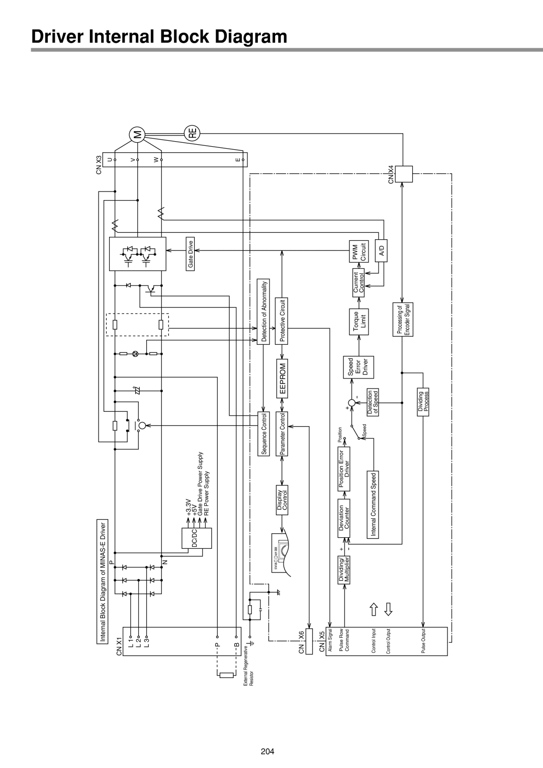
Internal Block Diagram of
P
CN X1
CN X3 |
U |
Driver Internal
L 1![]()
L 2![]()
L 3![]()
P
B
External Regenerative Resistor
N
DC/DC
+3.3V
+5V
Gate Drive Power Supply RE Power Supply
+ | V |
| W |
| Gate Drive |
E
M
RE
Block Diagram
204
Sequence Control |
| Detection of Abnormality |
|
|
|
Display | Parameter Control | EEPROM | Protective Circuit |
Control |
CN X6
CN X5
Alarm Signal
Pulse Row Command
Control Input
Control Output
Pulse Output
Dividing/ Multiplier
+
-
Deviation |
| Position Error |
Counter |
| Driver |
Internal Command Speed
Position
Speed
+
-
Detection of Speed
Dividing Process
Speed
Error
Driver
Torque | Current |
Limit | Control |
Processing of
Encoder Signal
PWM
Circuit
A/D
CN X4