Equipment Manual
Panel PC Computing Unit
Release 04/02
Safety Guidelines
Qualified Personnel
Trademarks
Correct Usage
Impressum
For your notes
Purpose
Preface
Documentation
History
Notation
Release Comments
Automation and Drives, Service & Support
Training Center
Simatic Customer Support Online Services
Other Sources of Assistance
Contents
Contents Release 04/02
Configuring the Computing Unit in Bios Setup
Release 04/02 Contents
Panel PC 670 Computing Unit, Equipment Manual
Chapter Overview
Product Overview
Section You Will Find
Computing unit
Installation
Advantages of the Computing Unit
Quality
Software equipment
Advantages of the computing unit
Safety Notes
Mains supply
For the USA and Canada
Power supply
Country-Specific Notes Repairs
Supply voltage outside the USA and Canada
Batteries
ESD guidelines
EMC guidelines
Certificates, Guidelines and Declarations
CE identification
Low voltage guidelines
Connection of periphery devices
Observe installation guidelines
DIN ISO 9001 certificate
Safety
Certification for USA, Canada and Australia
Conditions of Operations
Canada
Modifications
Canadian Notice
Australia
Starting Up the Computing Unit
Unpacking the computing unit
Unpacking and Checking the Computing Unit
Entering the production number SVP number
Installing the Computing Unit
297
Not permitted where a disk/CD-ROM/LS240 drive is installed
Position
Interfaces at bottom
Connection to the power supply
Ensuring Readiness for Service
Measures for equipotential
Connecting and switching on the computing unit
Switching the computing unit off
Transport
Shipping
Panel PC 670 Computing Unit, Equipment Manual
Connecting and Switching on Computing Unit
View of Interface Side
Ports
Release 04/02 Connecting and Switching on the Computing Unit
VGA interface
View of Drive Side
Connecting Periphery Units
Printer connection via the parallel interface
Connecting the Mouse
PS/2 mouse connection
Serial mouse connection
PS/2 Keyboard connection
USB device connection
USB connection ports
Working with PC Cards
PC cards
Examples of Pcmcia cards on the PC card interface for
Installation von PC cards
2 LS240 drive
Drives
Floppy disk drive
Disk types
Handling LS240 drive disks
Handling Floppy Disks
Emergency eject
Operation
Hard disk drive
CD-ROM drive or CD RW/DVD drive depending on unit equipment
Emergency eject
Backup Battery
Additional software
Point-to-point connection
Using the Computing Unit in a Simatic S5 Network
Rules
Connecting the computing unit to an S5 PLC
Connection to an S5 Programmable Controller
Connecting the computing unit via an adapter
Interface Connection Connecting cable Adapter
Connecting the computing unit to programming units TTY
10 Direction of Connection Adapter Connecting Cable
Connecting an S7 PLC via the MPI/DP interface
Using the Computing Unit in a Simatic S7 Network MPI/DP
Connection
MPI/PROFIBUS-DP network
How the network functions
Networking the Computing Unit and Other Nodes via Profibus
Networking the computing unit via Profibus
Hardware requirements
Connection Using Windows
Networking the computing unit via Industrial Ethernet
Panel PC 670 Computing Unit, Equipment Manual
Maintaining and Extending Computing Unit
Opening the Unit Conditions
Restricted liability
Before opening the device Tools
Opening the computing unit
Computing unit prepared for opening
Functional Units Visible After Opening the Device
View
Motherboard
Components on the motherboard
Number Functions
Standard memory
Installation of a Memory Extension
Memory Modules 64 MB 128 MB 256 MB
Installing the SO Dimm Modules
Battery voltage too low
Replacing the Backup Battery
Battery power supply for real-time clock and configuration
Replacing the battery
Changing Setup
Position of the backup battery
A31
Installation of Extension Modules
C18 A31
Short PCI card 5
Removing and installing the module retainer plates
10 Removing and installing an expansion board
Adjusting the module retainer plate
Removing and installing an ISA/PCI module
11 Removing and installing an expansion board
Removing and Installing Drives
Removing and installing the hard disk drive
13 Hard disk drive, with holder, removed
Removing and installing a CD-ROM drive
14 Computing unit with CD-ROM drive
Removing and installing the disk drive
15 Assembly of the computing unit floppy disk drive
Removing and installing the LS 240 drive
16 Assembly of the LS240 drive
Removing and Installing the Power Supply
17 Removing and installing the power supply
Removing and Installing the Bus Board
18 Removing and installing the bus board
Removing and Installing the Motherboard
19 Fixing screws on the motherboard
Removing and Installing the Fan
20 Removing and installing the fan
Processor Upgrade
21 Upgrading the processor
Reset button
22 Reset button
Panel PC 670 Computing Unit, Equipment Manual
Configuring the Computing Unit in Bios Setup
Boot Sequence Menu
Modifying the Device Configuration with Setup
Screen Display Following Power On
Menu items
Menu Meaning
Field Meaning
Setting in the Main Menu
Menu Main
By submenus
System Time und System Date Time and date
Floppy disk a Floppy disk drive
Field Type
Multi Sector Transfer field
Memory Cache Submenu
Write Back
Submenu Boot Options
QuickBoot Mode Enabled
Summary Screen
Submenu Keyboard Features
NumLock
Entry Meaning
Submenu Hardware Options
PCI-MPI/DP
CRT / LCD
Simultan
Settings of the Advanced menu
Menu structure
DOS
SubmenuCOM/LPT Configuration
Other
Printer Port Internal LPT1
Settable Mode Features Output Only
Bidirectional
PCI Configuration Submenu
PCI Devices Submenu
Submenu PCI/PNP ISA IRQ Resource Exclusion
IRQ Available
PCI IRQ line Field
AGP
Submenu Video Adapter Settings
PCI
3 Menü Security
Overview
Was entered during system boot
Menu Power
APM
Menu Boot-Sequence
19 Boot Sequence Menu Example
Menu Version
Menu Exit
Exit Menu
Documenting your device configuration
Setup default settings
System Parameters Standard Settings Your Entries
IRQ4
Security
Power
Boot Sequence
Version
Configure PC-Card interface
Fault Diagnosis
Cause
Problems Using External Modules
Fault screen
Remedy
External Screen Remains Dark
Cause/Remedy
Mouse driver not loaded
Display on the External Screen Does Not Appear or Scrolls
No Mouse Pointer Appears on the Screen/Display
Mouse not connected
Computing Unit Time and/or Date are Not Correct
USB Device Does Not Work
Error messages
Error Message Appears on the Screen/Display
Error message on screen Significance/Advice
Cmos
Beeps Hex Code
Computing Unit Self-Test Prior to Booting
Special codes
Example
Post codes
Display hex Meaning Description
Tpcacheconfig
Tpconfig
Tpquietbootstart
Tperrormsgs
Tpsetupchek
Tpenablenmi
Tppmsetup
Tperrorcheck
Panel PC 670 Computing Unit, Equipment Manual
Hardware Information
Basic system
Power Consumption of the Components Maximum Values
Sum max. for basic configuration 38 a 02 a
Component Voltage +5V +3.3V +12V
Overview of the Components and Interfaces
Component Port Description Parameters
Simatic S7
Component Description Parameters Port
USB
Start Programs Accessories System Tools System Information
System Resources
Overview
Signals on the front interface
Monitoring Functions
Function
Temperature monitoring
Temperature monitoring/display
Reaction Options
WD-Reaktionen
Watchdog WD
WD monitoring times TWD
Fan monitoring
External interfaces
Interfaces
Interface Position Connec Description Tor
Serial interface COM1 AG/V24/Modem
Pin No Short Name Meaning Input/Output
Serial interface COM2 V24/Mouse
Serial interface COM2 male
Parallel interface LPT1
PS/2 trackball keyboard interface
PS/2 mouse interface
Pin Short Name Meaning Input/Output
USB interface
VCC
MPI/DP interface
Pin Short Name Meaning Input/Output
Ethernet RJ45 connection
Symt
Exth
Pin Short Name Meaning Input Output
Ddcdat
Extv
Display port Cmos
Interface Posi Con Description Tion Nector
Vcon
Pin Signal
GND CLK
Enab
Display port Lvds
Pin No
Assignment of display to display select pins
Display type
Interface for front control elements
Internal serial interface COM2 V.24
Interface Position Connector Description
Assignment of internal interfaces on the mainboard
Pin No Short Name Meaning Input/Output
Interface to wiring backplane
Pspwrok
DC interface of the power supply 105W
Pin Short Name Meaning
P3V
Interface to floppy disk drive
Allocation of IDE intefaces
Pin X41 Meaning X4/X3
Hdactn
Connection of an LS240 drive
CSN
CS1N
Connection for CPU fan
Connection for buffer battery
SV connection for hard disk
Connection for device fan
Pin assignmentI SA slot
Wiring Backplane Design and Theory of Operation
Pin No Short Name Type
IOR#
SMEMR#
IOW#
DACK3#
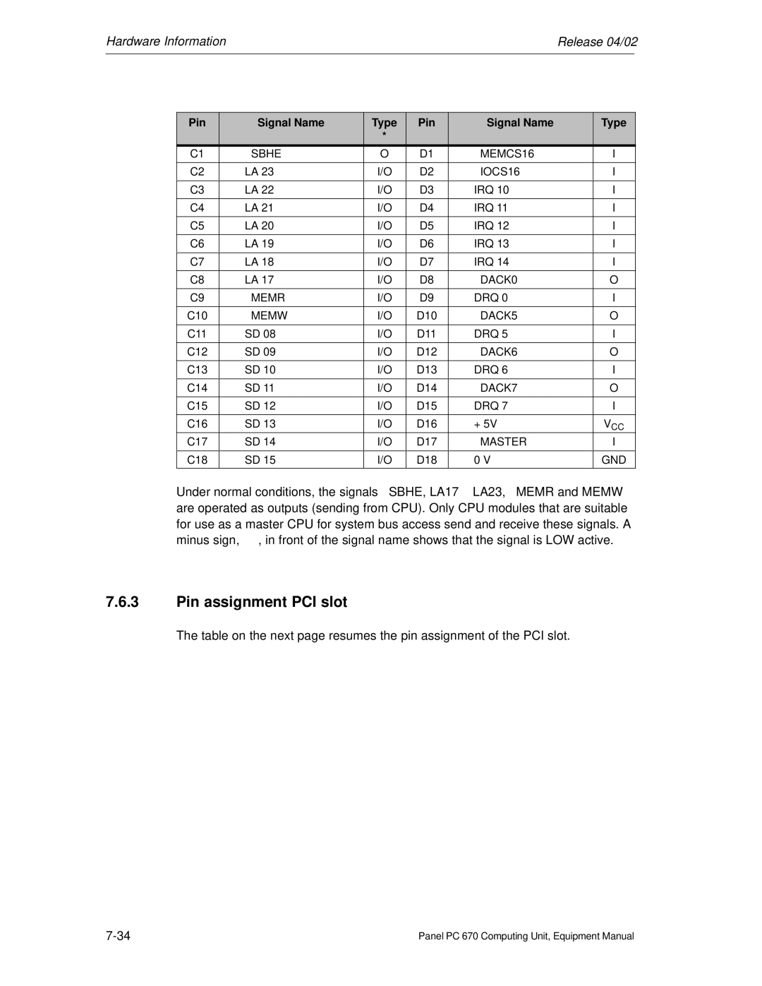
Pin Signal Name Type
Pin assignment PCI slot
5V System Environment
5V System Environment Side B Side a
Side B Side a
Assignment of slot-specific PCI bus signals
PCI Socket PCI Slot Shared ISA PCI Slot Pin No
Power-Good-Signal
Power supply AC and DC
Technical Data
Voltage
Simatic S5 Connecting Cable
Connecting cables
Simatic S7 Connecting Cable for MPI/DP
Distributed configuration
Description
Mounting
Dimensions
Mounting positions
Cable connection
Display codes
Computing
Transmitter housing
Unit
Type Resolutio S30/4 S30/3 S30/2 S30/1
Panel PC 670 Computing Unit, Equipment Manual
Technical Data
This Appendix
General
Technical Data of the Panel PC 670 Computing Unit
Electromagnetic compatibility EMC
Mechanical environmental conditions
Special Features
Environmental conditions
Mainboard
Interfaces
Graphic
Function displays light-emitting diodes on device
ESD Guidelines
Chapter You Will Find
What does ESD mean?
Definition
Electrostatic Charge of People
Charging
Ensuring a good ground connection
Avoid direct contact
Structure of the documentation
Simatic HMI Documentation
Target groups
Overview of complete documentation
Documentation Target Group Content
Simatic HMI Documentation Release 04/02
Release 04/02 Simatic HMI Documentation
Simatic
Simatic S5
Simotion
Glossary
COM2 port
Drivers
Configuration software
Device configuration
Ethernet port
LPT 1 port
Interrupt
Keyboard port
LS 120 drive
PC card interface
MPI/DP port
Parallel port
PCI or PCI/ISA slot
TFT display
Setup Bios Setup
Scsi interface
USB port
Panel PC 670 Computing Unit, Equipment Manual
Index
Index Release 04/02
Release 04/02 Index
Profibus
Index-5
Panel PC 670 Computing Unit, Equipment Manual