ANY-FREQUENCY Precision Clocks
Si53xx-RM
Table of Contents
Output Clock Drivers
High-Speed I/O
Si5375 Free Run Mode
Si53xx-RM
List of Figures
Differential Output Example Requiring Attenuation 108
Si53xx-RM
List of Tables
Si53xx-RM
Any-Frequency Precision Clock Product Family Overview
Si53xx-RM
PLL
Product Selection Guide
Device
Product Selection Guide Si5322/25/65/67
Precision Clock Multipliers Wideband
Narrowband vs. Wideband Overview
Si5316
Any-Frequency Clock Family Members
Dspll
Si5319
Si5322
Si5322 Low Jitter Clock Multiplier Block Diagram
Si5323
Si5323 Jitter Attenuating Clock Multiplier Block Diagram
Si5324
Si5324 Clock Multiplier and Jitter Attenuator Block Diagram
Si5325
Si5325 Low Jitter Clock Multiplier Block Diagram
Si5326
Si5326 Clock Multiplier and Jitter Attenuator Block Diagram
Si5327
Si5327 Clock Multiplier and Jitter Attenuator Block Diagram
Si5365
Si5365 Low Jitter Clock Multiplier Block Diagram
10. Si5366
Si5366 Jitter Attenuating Clock Multiplier Block Diagram
11. Si5367
Si5367 Clock Multiplier Block Diagram
12. Si5368
Si5368 Clock Multiplier and Jitter Attenuator Block Diagram
14. Si5374/75 Compared to Si5324/19
13. Si5369
15. Si5374
Si5374 Functional Block Diagram
16. Si5375
Si5375 Functional Block Diagram
Parameter Symbol Test Condition
Device Specifications
Recommended Operating Conditions1
Min Typ Max Unit
CKINn Input Pins
DC Characteristics
Lvpecl 100 Ω
Level Input Pins
Level Lvcmos Input Pins
RST
Lvcmos Output Pins
Parameter Symbol Test Conditions Min Typ Max Unit
SPI Specifications Si5324, Si5325, Si5367, and Si5368
SDO
Differential Reference Clock Input Pins XA/XB
Frame Synchronization Timing
Min Typ Max Units
AC Characteristics-All Devices
Lvcmos Pins
PLL Performance
Device Skew
Ckopn
Jitter Generation Si5322, Si5325, Si5365, Si5367
Jitter Generation Si5316, Si5324, Si5366, Si5368
Parameter Symbol Test Condition Devices Value Unit
Thermal Characteristics
Dspll All Devices
Any-Frequency Precision Clock Dspll Block Diagram
Clock Multiplication Circuit
Clock Multiplication
Jitter Generation
PLL Performance
Jitter Transfer
Jitter Tolerance
Jitter Tolerance Mask/Template
Frequency Settings
Si5316, Si5322, Si5323, Si5365 and Si5366 Key Features
Pin Control Parts Si5316, Si5322, Si5323, Si5365, Si5366
Clock Multiplication Si5316, Si5322, Si5323, Si5365, Si5366
Si5316 Bandwidth Values
Input Divider Settings
CKnDIV N3n Input Divider
FRQSEL10 Nominal Frequency Values MHz BW10
Clock Multiplication Si5322, Si5323, Si5365, Si5366
Sonet Clock Multiplication Settings FRQTBL=L
Fsout MHz
Ckconf =
All Devices Si5366 Only FOUT MHz
FIN MHz Mult Factor
Mllm
Hlll
Hhlh
Setting
Datacom Clock Multiplication Settings Frqtbl = M, Ckconf =
MHz Mult Factor OUT* MHz
125 10/8 x 66/64 161.13
173.37 X 64/66 x 237/255 125
Hhhl
FIN MHz Mult Factor FOUT* MHz
Sonet to Datacom Clock Multiplication Settings
62.500 125
155.520 15625/15552 156.25
CKOUT3 and CKOUT4 Si5365 and Si5366
Clock Output Divider Control DIV34
Lock Detect Si5322 and Si5365
Input-to-Output Skew Si5322 and Si5365
PLL Self-Calibration
Si5365 and Si5366 Pins and Reset
Si5316, Si5322, and Si5323 Pins and Reset
Manual Input Clock Selection Si5365, Si5366, Autosel = L
Pin Control Input Clock Control
Clock Active Indicators Autosel = M or H Si5365 and Si5367
Clock Active Indicators Autosel = M or H Si5322 and Si5323
Input Clock Priority for Auto Switching Si5322, Si5323
Automatic/Manual Clock Selection
Hitless Switching with Phase Build-Out Si5323, Si5366
Input Clock Priority for Auto Switching Si5365, Si5366
Digital Hold/VCO Freeze
Recovery from Digital Hold Si5316, Si5323, Si5366
Frame Synchronization Si5366
Narrowband Digital Hold Si5316, Si5323, Si5366
Using Fsout as a Fifth Output Clock Si5366
Output Phase Adjust Si5323, Si5366
Fsync Realignment Si5366
Including Fsync Inputs in Clock Selection Si5366
Output Signal Format Selection Sfout
Fsout Disable Control Dblfs
Output Clock Drivers
Alarms
PLL Bypass Mode
DSBL2/BYPASS Pin Settings
Frequency Offset Control Fosctl
Alarm Output Logic Equations
DSPLLsim Configuration Software
Device Reset
Lock Detect Retrigger Time
Wideband PLL Divider Settings Si5325, Si5367
Lock Detect Si5325, Si5367
Loop Bandwidth Si5325, Si5367
Input to Output Skew Si5325, Si5367
Dividers and Limits
Signal Frequency Limits
Low Loop Bandwidth Si5324, Si5327, Si5369, Si5374
Loop Bandwidth Si5319, Si5326, Si5368, Si5375
Initiating Internal Self-Calibration
Ckoutalwayson and Sqical Truth Table
Input Clock Control
Input Clock Configurations Si5367 and Si5368
Active Input Clock
Manual Input Clock Selection Si5367, Si5368, Si5369
Register Bits
CKIN1,2,3,4 inputs CKIN1,3 & CKIN2,4 clock/FSYNC pairs
Ckselreg or CS pin Active Input Clock
Manual Input Clock Selection Si5324, Si5325, Si5326, Si5374
Selected Clock
Input Clock Priority for Auto Switching
Clock Control Logic in Free Run Mode
Free Run Mode Programming Procedure
While in Free Run
Free Run Reference Frequency Constraints
Parameters in History Value of M
Digital Hold
Digital Hold History Averaging Time
Digital Hold History Delay
Digital Hold versus VCO Freeze
VCO Freeze Si5319, Si5325, Si5367, Si5375
Unlimited Coarse Skew Adjustment Si5326, Si5368
Output Phase Adjust Si5326, Si5368
Coarse Skew Control Si5326, Si5368
Fine Skew Control Si5326, Si5368
Output Phase Adjust Si5324, Si5327, Si5369, Si5374
Frame Synchronization Realignment Si5368 and Ckconfigreg =
Independent Skew Si5324, Si5326, Si5368, Si5369, Si5374
Input-to-Output Skew All Devices
CKINn Frequency kHz Divisor
CKIN3/CKIN4 Frequency Selection Ckconf =
Alignment Alarm Trigger Threshold
Common NC5 Divider Settings
CKOUT2 Frequency MHz NC5 Divider Setting KHz Fsout
Alarm Trigger Threshold Units of T CKOUT2
Fsync Skew Control Si5368
Using Fsout as a Fifth Output Clock Si5368
Including Fsync Inputs in Clock Selection Si5368
Fsout Polarity and Pulse Width Control Si5368
Disabling CKOUTn
Output Signal Format Selection
Loss-of-Signal Registers
Loss-of-Signal Validation Times
Clock Validation Time
LOS Selection
FOS Algorithm Si5324, Si5325, Si5326, Si5368, Si5369, Si5374
CLKnRATE Registers
FOS Reference Clock Selection
FOS Reference
Si5326 Si5368
Fosen
LOS Si5319, Si5375
11.6. C1B, C2B, C3B, Alrmout Si5368 Ckconfigreg =
Alarm Output Logic Equations Si5368 and Ckconfigreg =
Device Interrupts
Lock Detect Retrigger Time Lockt
13. I2C Serial Microprocessor Interface
I2C Command Format
Serial Microprocessor Interface SPI
SPI Command Format
InstructionBYTE0 Address/Data70BYTE1
Register Descriptions
Default Device Configuration
Input Clock Buffers
High-Speed I/O
CML/LVDS Termination 1.8, 2.5, 3.3
Typical Output Circuits
Output Driver Configuration
Output Driver Si5365, Si5366 Si5325, Si5326, Si5367, Si5368
Disabling Unused Output Driver
Typical Clock Output Scope Shots
Output Format Measurements1,2
Name Sfout Pin Sfout Code Single Diff Vocm Vpk-pk
Sfout3, lowSwingLVDS
Sfout2, Cmos
Sfout5, Lvpecl
Sfout7, Lvds
Cmos External Reference Circuit
OSC-P
Parameter Symbol Min Max
Three-Level 3L Input Pins No External Resistors
Three-Level 3L Input Pins With External Resistors
Typical Power Supply Bypass Network Tqfp Package
Power Supply
Packages and Ordering Guide
Approved Crystals
Resonator/External Clock Selection
XA/XB Reference Sources and Frequencies
RATE10
Reference Jitter
Fundamental Mode Crystals Reference Drift
38.88MHz XO, 38.88MHz CKIN, 38.88MHz Ckout
Phase
Phase Noise versus f3, 155.52 MHz in, 622.08 MHz out
High f3 Value
DBc/Hz Noise
Offset Frequency Hz
MHz in, 622.08 MHz out, 696.399 MHz out
Reference vs. Output Frequency
Yellow-696.399 MHz output Blue-622.08 MHz output
MHz Out Jitter Bandwidth Yellow, fs RMS Blue, fs RMS
MHz thru 163 MHz Ext Ref, 155.52 MHz in, 622.08 MHz out
High Reference Frequency
SONETOC192A, 20 kHz to 80 MHz
MHz thru 180 MHz Ext Ref, 155.52 MHz in, 622.08 MHz out
SONETOC192B, 4 MHz to 80 MHz
SONETOC192C, 50 kHz to 80 MHz
Appendix C-TYPICAL Phase Noise Plots
52 MHz In 622.08 MHz Out Loop BW = 7 Hz, Si5324
44 MHz In 156.25 MHz Out Loop BW = 80 Hz
44 MHz In 156.25 MHz Out Loop BW = 5 Hz, Si5324
130
44 MHz In 491.52 MHz Out Loop BW = 7 Hz, Si5324
08 MHz In 672.16 MHz Out Loop BW = 6.9 kHz
08 MHz In 672.16 MHz Out Loop BW = 100 Hz
25 MHz In 155.52 MHz Out
Jitter Bandwidth 644.531 MHz Jitter RMS
125 MHz In 644.531 MHz Out Jitter Values for Figure
Jitter Bandwidth 690.569 MHz Jitter RMS
125 MHz In 690.569 MHz Out Jitter Values for Figure
Jitter Bandwidth 693.493 MHz Jitter RMS
125 MHz In 693.493 MHz Out Jitter Values for Figure
DBc/Hz
MHz in, 173.371 MHz and 693.493 MHz out
Offset Frequency Hz
Jitter Values for Figure
685 MHz In 173.371 MHz Out
685 MHz In 693.493 MHz Out
DBc/Hz
MHz and 156.25MHz in, 622.08 MHz out
Jitter Bandwidth MHz Input Jitter RMS
MHz In 1 GHz Out
MHz in, 148.5 MHz out
Digital Video HD-SDI
Jitter Band
Appendix D-ALARM Structure
Si5368 Alarm Diagram 1
Si5368 Alarm Diagram 2
Si5322 Pullup/Down
Si5316 Pullup/Down
Pin # Si5316 Pull?
Pin # Si5322 Pull?
Si5319, Si5324, Pullup/Down
Si5323 Pullup/Down
Pin # Si5323 Pull?
Pin # Si5326 Pull?
Si5326 Pullup/Down
Si5325 Pullup/Down
Pin # Si5325 Pull?
Si5365 Pullup/Down
Si5327 Pullup/Down
Pin # Si5327 Pull?
Pin # Si5365 Pull?
Pin # Si5366 Pull?
Si5366 Pullup/Down
Si5368 Pullup/Down
Si5367 Pullup/Down
Pin # Si5367 Pull?
Pin # Si5368 Pull?
Si5374/75 Pullup/Down
Si5369 Pullup/Down
Pin # Si5374/75 Pull?
MHz in, 622.08 MHz out
Bypass 622.08 MHz In, 622.08 MHz Out
Power Supply Noise to Output Transfer Function
Power Supply Noise Rejection
MHz in, 155.52 MHz out Bandwidth = 110 Hz
Jitter Band MHz MHz out 622.084 MHz
Clock Input Crosstalk Results Test Conditions
Out No crosstalk 155.52 MHz
Hz loop KHz loop
5 .5 2 1 M H z in , 6 2 2 .0 8 4 M H z o u t
Clock Input Crosstalk Phase Noise Plots
155 .521 MHz in, 622 .084 MHz ou t
Clock Input Crosstalk Detail View
155 .521 M H z in, 622.084 M H z out
Clock Input Crosstalk Wideband Comparison
Clock Input Crosstalk Output of Rohde and Schwartz RF
Spectrum Analyzer Agilent Model E444OA
Jitter vs. Output Format 19.44 MHz In, 622.08 MHz Out
Output Format vs. Jitter
Hz in, 622.08 M Hz out
Input Frequency Variation = ±50 ppm
Test Conditions
MHz External XA-XB Reference
Jitter, fs
Input Frequency Variation = ±2000 ppm
Input Frequency
Fmod Fdev Jitter Start RF Gen Si5326 Si5324
Jitter Values
RF Generator, Si5326, Si5324 No Jitter For Reference
MHz in, 622.08 MHz out
RF Generator, Si5326, Si5324 100 Hz Jitter
RF Generator, Si5326, Si5324 1 kHz Jitter
RF Generator, Si5326, Si5324 10 kHz Jitter
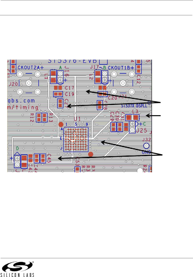
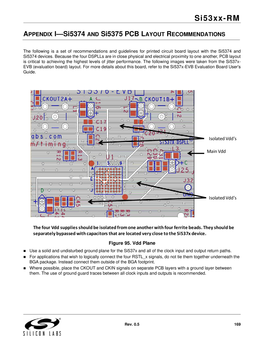
Appendix I-Si5374AND Si5375 PCB Layout Recommendations
Ground Plane and Reset
Output Clock Routing
Oscp Oscn
Si5374/75 Crosstalk Jitter Values
Si5374, Si5375 Crosstalk Test Bed
Jitter, fsec RMS
Si5374, Si5375 Dspll a
Si5374, Si5375 Dspll B
Si5374, Si5375 Dspll C
Si5374, Si5375 Dspll D
Revision 0.4 to Revision
Revision 0.3 to Revision
Revision 0.41 to Revision
Revision 0.42 to Revision
Rev 179
Contact Information