www.ti.com | Peripheral Architecture |
The prescaler (IPSC bit in ICPSC) must only be initialized while the I2C module is in the reset state (IRS = 0 in ICMDR). The prescaled frequency only takes effect when the IRS bit in ICMDR is changed to
1. Changing the IPSC bit in ICPSC while IRS = 1 in ICMDR has no effect. Likewise, you must configure the I2C clock dividers (ICCH bit in ICCLKH and ICCL bit in ICCLKL) while the I2C module is still in reset (IRS = 0 in ICMDR).
2.3Clock Synchronization
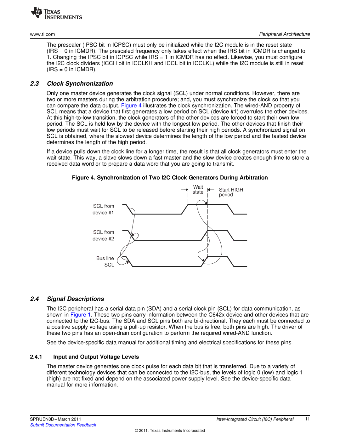
Only one master device generates the clock signal (SCL) under normal conditions. However, there are two or more masters during the arbitration procedure; and, you must synchronize the clock so that you can compare the data output. Figure 4 illustrates the clock synchronization. The
If a device pulls down the clock line for a longer time, the result is that all clock generators must enter the wait state. This way, a slave slows down a fast master and the slow device creates enough time to store a received data word or to prepare a data word that you are going to transmit.
Figure 4. Synchronization of Two I2C Clock Generators During Arbitration
Wait state
SCL from device #1
SCL from device #2
Bus line
SCL
Start HIGH period
2.4Signal Descriptions
The I2C peripheral has a serial data pin (SDA) and a serial clock pin (SCL) for data communication, as shown in Figure 1. These two pins carry information between the C642x device and other devices that are connected to the
See the
2.4.1Input and Output Voltage Levels
The master device generates one clock pulse for each data bit that is transferred. Due to a variety of different technology devices that can be connected to the
SPRUEN0D | 11 | |
Submit Documentation Feedback |
|
|
© 2011, Texas Instruments Incorporated