www.ti.com | Peripheral Architecture |
2Peripheral Architecture
The I2C peripheral consists of the following primary blocks:
•A serial interface: one data pin (SDA) and one clock pin (SCL)
•Data registers to temporarily hold receive data and transmit data traveling between the SDA pin and the CPU or the EDMA controller
•Control and status registers
•A peripheral data bus interface to enable the CPU and the EDMA controller to access the I2C peripheral registers
•A clock synchronizer to synchronize the I2C input clock (from the processor clock generator) and the clock on the SCL pin, and to synchronize data transfers with masters of different clock speeds
•A prescaler to divide down the input clock that is driven to the I2C peripheral
•A noise filter on each of the two pins, SDA and SCL
•An arbitrator to handle arbitration between the I2C peripheral (when it is a master) and another master
•Interrupt generation logic, so that an interrupt can be sent to the CPU
•EDMA event generation logic, so that activity in the EDMA controller can be synchronized to data reception and data transmission in the I2C peripheral
Figure 1 shows the four registers used for transmission and reception. The CPU or the EDMA controller writes data for transmission to ICDXR and reads received data from ICDRR. When the I2C peripheral is configured as a transmitter, data written to ICDXR is copied to ICXSR and shifted out on the SDA pin one bit a time. When the I2C peripheral is configured as a receiver, received data is shifted into ICRSR and then copied to ICDRR.
2.1Bus Structure
Figure 1 shows how the I2C peripheral is connected to the I2C bus. The I2C bus is a multi-master bus that supports a multi-master mode. This allows more than one device capable of controlling the bus that is connected to it. A unique address recognizes each I2C device. Each I2C device can operate as either transmitter or receiver, depending on the function of the device. Devices that are connected to the I2C bus can be considered a master or slave when performing data transfers, in addition to being a transmitter or receiver.
NOTE: A master device is the device that initiates a data transfer on the bus and generates the clock signals to permit that transfer. Any device that is addressed by this master is considered a slave during this transfer.
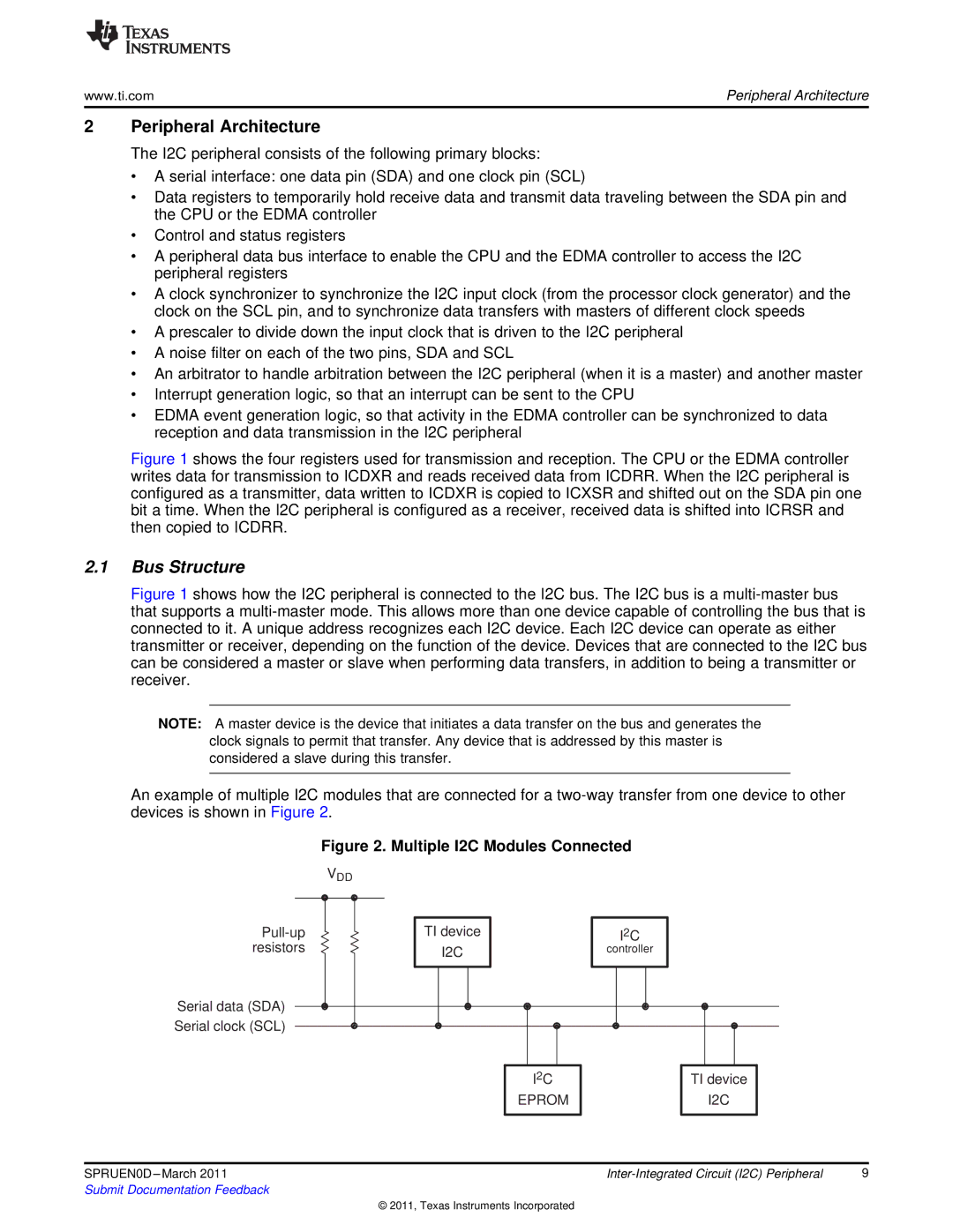
An example of multiple I2C modules that are connected for a two-way transfer from one device to other devices is shown in Figure 2.
Figure 2. Multiple I2C Modules Connected
VDD
Serial data (SDA) Serial clock (SCL)
TI device |
|
| I2C | |||
| I2C |
| controller | |||
|
|
|
|
|
|
|
|
|
|
|
|
|
|
|
|
|
|
|
|
|
I2C |
| TI device |
EPROM |
| I2C |
|
|
|
SPRUEN0D | 9 | |
Submit Documentation Feedback |
|
|
© 2011, Texas Instruments Incorporated