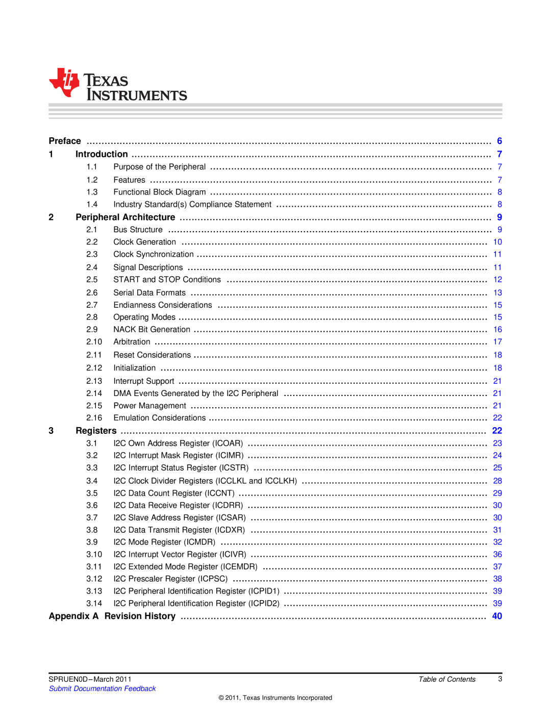
Preface | 6 | ||
1 | Introduction | 7 | |
| 1.1 | Purpose of the Peripheral | 7 |
| 1.2 | Features | 7 |
| 1.3 | Functional Block Diagram | 8 |
| 1.4 | Industry Standard(s) Compliance Statement | 8 |
2 | Peripheral Architecture | 9 | |
| 2.1 | Bus Structure | 9 |
| 2.2 | Clock Generation | 10 |
| 2.3 | Clock Synchronization | 11 |
| 2.4 | Signal Descriptions | 11 |
| 2.5 | START and STOP Conditions | 12 |
| 2.6 | Serial Data Formats | 13 |
| 2.7 | Endianness Considerations | 15 |
| 2.8 | Operating Modes | 15 |
| 2.9 | NACK Bit Generation | 16 |
| 2.10 | Arbitration | 17 |
| 2.11 | Reset Considerations | 18 |
| 2.12 | Initialization | 18 |
| 2.13 | Interrupt Support | 21 |
| 2.14 | DMA Events Generated by the I2C Peripheral | 21 |
| 2.15 | Power Management | 21 |
| 2.16 | Emulation Considerations | 22 |
3 | Registers | 22 | |
| 3.1 | I2C Own Address Register (ICOAR) | 23 |
| 3.2 | I2C Interrupt Mask Register (ICIMR) | 24 |
| 3.3 | I2C Interrupt Status Register (ICSTR) | 25 |
| 3.4 | I2C Clock Divider Registers (ICCLKL and ICCLKH) | 28 |
| 3.5 | I2C Data Count Register (ICCNT) | 29 |
| 3.6 | I2C Data Receive Register (ICDRR) | 30 |
| 3.7 | I2C Slave Address Register (ICSAR) | 30 |
| 3.8 | I2C Data Transmit Register (ICDXR) | 31 |
| 3.9 | I2C Mode Register (ICMDR) | 32 |
| 3.10 | I2C Interrupt Vector Register (ICIVR) | 36 |
| 3.11 | I2C Extended Mode Register (ICEMDR) | 37 |
| 3.12 | I2C Prescaler Register (ICPSC) | 38 |
| 3.13 | I2C Peripheral Identification Register (ICPID1) | 39 |
| 3.14 | I2C Peripheral Identification Register (ICPID2) | 39 |
Appendix A | Revision History | 40 | |
SPRUEN0D | Table of Contents | 3 |
Submit Documentation Feedback |
|
|
© 2011, Texas Instruments Incorporated
