www.ti.com
Peripheral Architecture
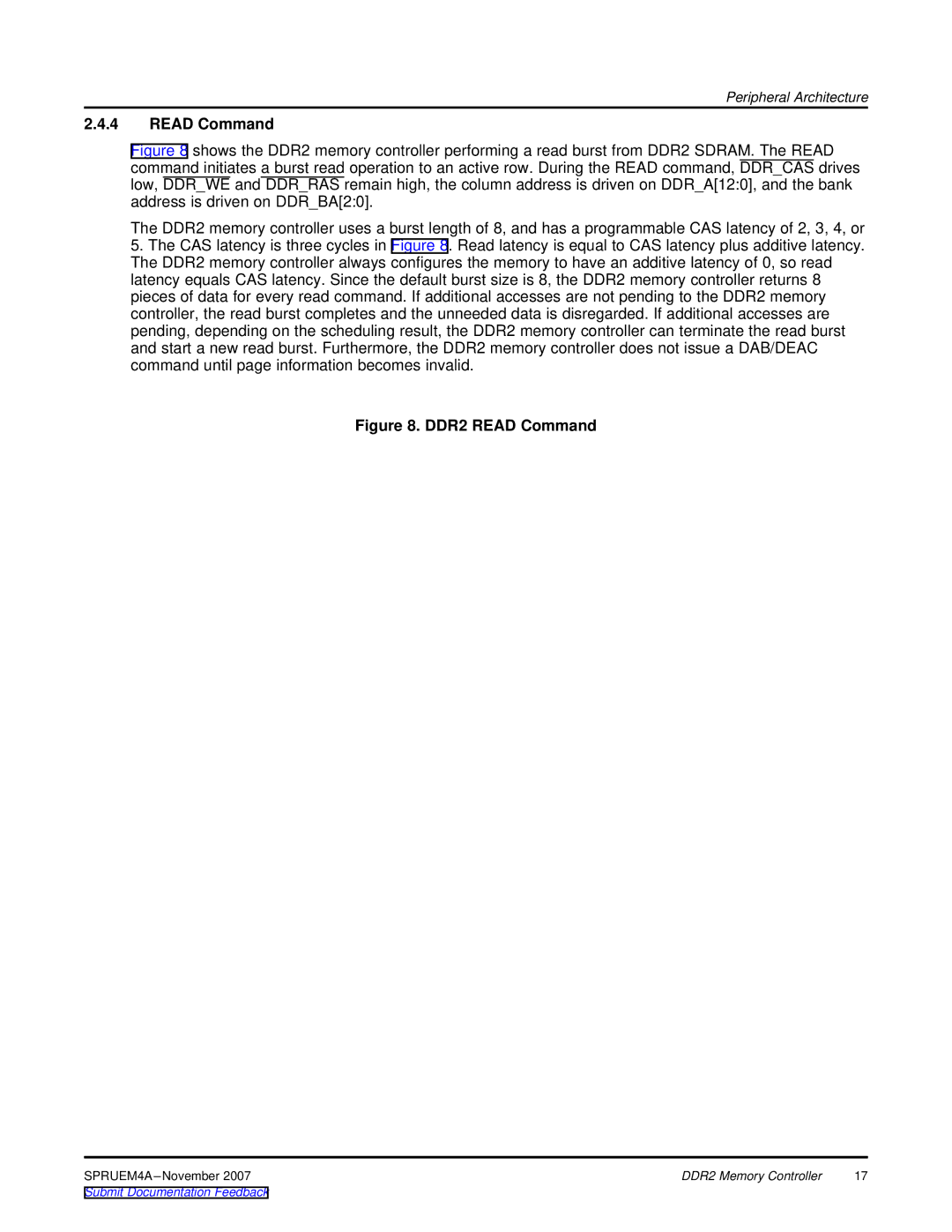
2.4.4READ Command
Figure 8 shows the DDR2 memory controller performing a read burst from DDR2 SDRAM. The READ command initiates a burst read operation to an active row. During the READ command, DDR_CAS drives low, DDR_WE and DDR_RAS remain high, the column address is driven on DDR_A[12:0], and the bank address is driven on DDR_BA[2:0].
The DDR2 memory controller uses a burst length of 8, and has a programmable CAS latency of 2, 3, 4, or
5.The CAS latency is three cycles in Figure 8. Read latency is equal to CAS latency plus additive latency. The DDR2 memory controller always configures the memory to have an additive latency of 0, so read latency equals CAS latency. Since the default burst size is 8, the DDR2 memory controller returns 8 pieces of data for every read command. If additional accesses are not pending to the DDR2 memory controller, the read burst completes and the unneeded data is disregarded. If additional accesses are pending, depending on the scheduling result, the DDR2 memory controller can terminate the read burst and start a new read burst. Furthermore, the DDR2 memory controller does not issue a DAB/DEAC command until page information becomes invalid.
Figure 8. DDR2 READ Command
DDR_CLK
DDR_CLK
DDR_CKE
DDR_CS
DDR_RAS
DDR_CAS
DDR_WE
DDR_A[12:0] ![]() COL
COL ![]()
DDR_BA[2:0] ![]() BANK
BANK ![]()
DDR_A[10]
DDR_DQM[3:0]
CAS Latency
DDR_D[31:0] | D0 | D1 | D2 | D3 | D4 | D5 | D6 | D7 |
DDR_DQS[3:0]
DDR2 Memory Controller | 17 |