Texas Instruments TMS320C642x DSP manual Functional Block Diagram, Supported Use Case Statement

Models: TMS320C642x DSP

1 57
Download 57 pages 6.18 Kb
Page 8
Image 8
1.3Functional Block Diagram

www.ti.com

Introduction

1.3Functional Block Diagram

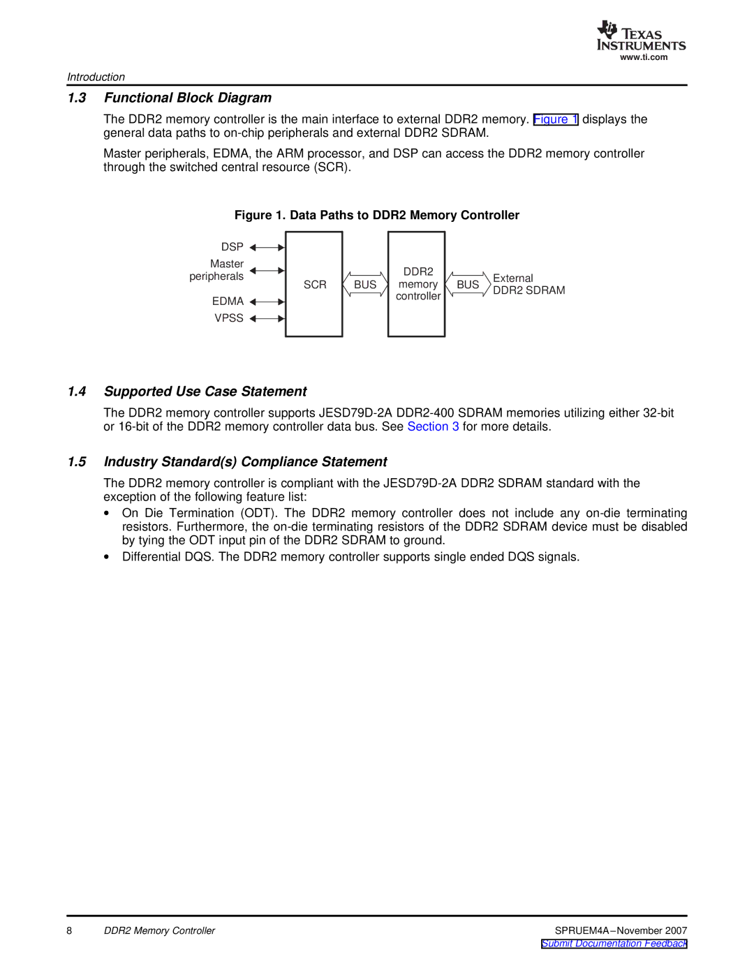
The DDR2 memory controller is the main interface to external DDR2 memory. Figure 1 displays the general data paths to on-chip peripherals and external DDR2 SDRAM.

Master peripherals, EDMA, the ARM processor, and DSP can access the DDR2 memory controller through the switched central resource (SCR).

Figure 1. Data Paths to DDR2 Memory Controller

DSP Figure 1. Data Paths to DDR2 Memory Controller

Master peripherals

EDMA 1.4Supported Use Case Statement1.5Industry Standard(s) Compliance Statement VPSS Manual backgroundManual background

SCR

Manual background BUS Manual background

DDR2

memory controller

Manual backgroundManual background External

BUS DDR2 SDRAM

1.4Supported Use Case Statement

The DDR2 memory controller supports JESD79D-2A DDR2-400 SDRAM memories utilizing either 32-bit or 16-bit of the DDR2 memory controller data bus. See Section 3 for more details.

1.5Industry Standard(s) Compliance Statement

The DDR2 memory controller is compliant with the JESD79D-2A DDR2 SDRAM standard with the exception of the following feature list:

On Die Termination (ODT). The DDR2 memory controller does not include any on-die terminating resistors. Furthermore, the on-die terminating resistors of the DDR2 SDRAM device must be disabled by tying the ODT input pin of the DDR2 SDRAM to ground.

Differential DQS. The DDR2 memory controller supports single ended DQS signals.

8

DDR2 Memory Controller

SPRUEM4A–November 2007

Submit Documentation Feedback

Page 8
Image 8
Texas Instruments TMS320C642x DSP manual Functional Block Diagram, Supported Use Case Statement