www.ti.com
DDR2 Memory Controller Registers
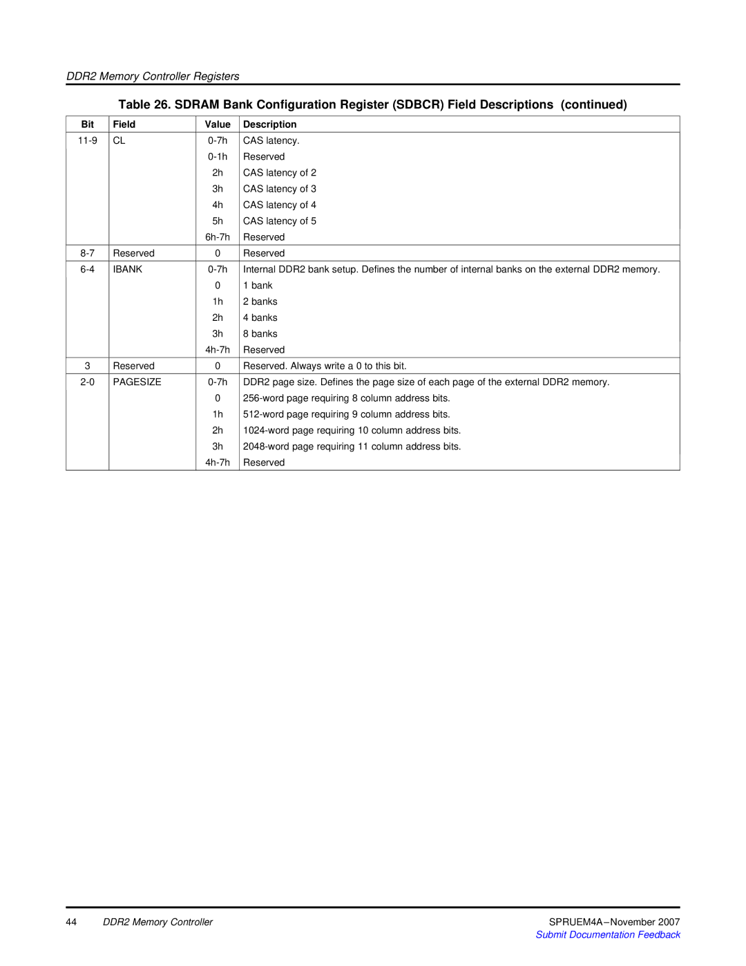
Table 26. SDRAM Bank Configuration Register (SDBCR) Field Descriptions (continued)
Bit | Field | Value | Description |
CL | CAS latency. | ||
|
| Reserved | |
|
| 2h | CAS latency of 2 |
|
| 3h | CAS latency of 3 |
|
| 4h | CAS latency of 4 |
|
| 5h | CAS latency of 5 |
|
| Reserved | |
Reserved | 0 | Reserved | |
IBANK | Internal DDR2 bank setup. Defines the number of internal banks on the external DDR2 memory. | ||
|
| 0 | 1 bank |
|
| 1h | 2 banks |
|
| 2h | 4 banks |
|
| 3h | 8 banks |
|
| Reserved | |
3 | Reserved | 0 | Reserved. Always write a 0 to this bit. |
PAGESIZE | DDR2 page size. Defines the page size of each page of the external DDR2 memory. | ||
|
| 0 | |
|
| 1h | |
|
| 2h | |
|
| 3h | |
|
| Reserved |
44 | DDR2 Memory Controller | |
|
| Submit Documentation Feedback |