www.ti.com
Peripheral Architecture
2.7Address Mapping
The DDR2 memory controller views external DDR2 SDRAM as one continuous block of memory. This statement is true regardless of the number of external physical devices mapped to a given chip select space. The DDR2 memory controller receives DDR2 memory access requests along with a
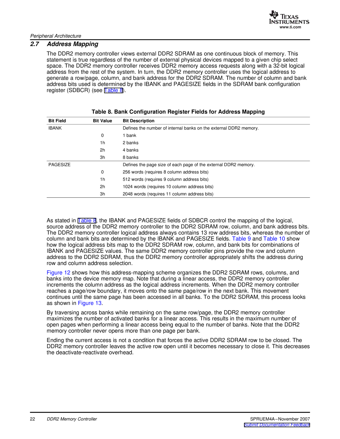
Table 8. Bank Configuration Register Fields for Address Mapping
Bit Field | Bit Value | Bit Description |
IBANK |
| Defines the number of internal banks on the external DDR2 memory. |
| 0 | 1 bank |
| 1h | 2 banks |
| 2h | 4 banks |
| 3h | 8 banks |
PAGESIZE |
| Defines the page size of each page of the external DDR2 memory. |
| 0 | 256 words (requires 8 column address bits) |
| 1h | 512 words (requires 9 column address bits) |
| 2h | 1024 words (requires 10 column address bits) |
| 3h | 2048 words (requires 11 column address bits) |
As stated in Table 8, the IBANK and PAGESIZE fields of SDBCR control the mapping of the logical, source address of the DDR2 memory controller to the DDR2 SDRAM row, column, and bank address bits. The DDR2 memory controller logical address always contains 13 row address bits, whereas the number of column and bank bits are determined by the IBANK and PAGESIZE fields. Table 9 and Table 10 show how the logical address bits map to the DDR2 SDRAM row, column, and bank bits for combinations of IBANK and PAGESIZE values. The same DDR2 memory controller pins provide the row and column address to the DDR2 SDRAM, thus the DDR2 memory controller appropriately shifts the address during row and column address selection.
Figure 12 shows how this address-mapping scheme organizes the DDR2 SDRAM rows, columns, and banks into the device memory map. Note that during a linear access, the DDR2 memory controller increments the column address as the logical address increments. When the DDR2 memory controller reaches a page/row boundary, it moves onto the same page/row in the next bank. This movement continues until the same page has been accessed in all banks. To the DDR2 SDRAM, this process looks as shown in Figure 13.
By traversing across banks while remaining on the same row/page, the DDR2 memory controller maximizes the number of activated banks for a linear access. This results in the maximum number of open pages when performing a linear access being equal to the number of banks. Note that the DDR2 memory controller never opens more than one page per bank.
Ending the current access is not a condition that forces the active DDR2 SDRAM row to be closed. The DDR2 memory controller leaves the active row open until it becomes necessary to close it. This decreases the deactivate-reactivate overhead.
22 | DDR2 Memory Controller |