www.ti.com
DDR2 Memory Controller Registers
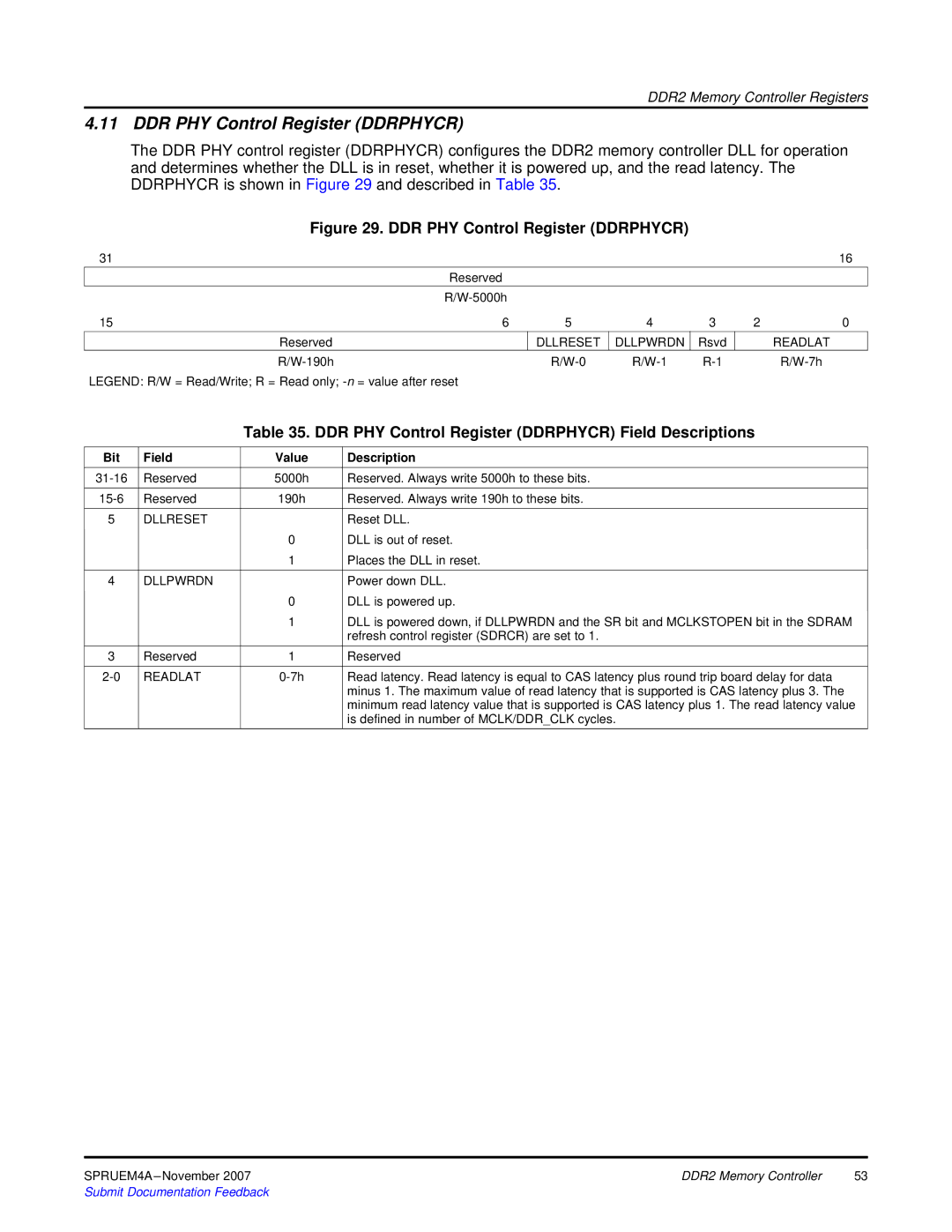
4.11 DDR PHY Control Register (DDRPHYCR)
The DDR PHY control register (DDRPHYCR) configures the DDR2 memory controller DLL for operation and determines whether the DLL is in reset, whether it is powered up, and the read latency. The DDRPHYCR is shown in Figure 29 and described in Table 35.
Figure 29. DDR PHY Control Register (DDRPHYCR)
31 |
|
|
|
|
| 16 |
| Reserved |
|
|
|
|
|
|
|
|
|
|
| |
15 | 6 | 5 | 4 | 3 | 2 | 0 |
Reserved |
| DLLRESET | DLLPWRDN | Rsvd |
| READLAT |
|
|
LEGEND: R/W = Read/Write; R = Read only;
Table 35. DDR PHY Control Register (DDRPHYCR) Field Descriptions
Bit | Field | Value | Description |
Reserved | 5000h | Reserved. Always write 5000h to these bits. | |
Reserved | 190h | Reserved. Always write 190h to these bits. | |
5 | DLLRESET |
| Reset DLL. |
|
| 0 | DLL is out of reset. |
|
| 1 | Places the DLL in reset. |
4 | DLLPWRDN |
| Power down DLL. |
|
| 0 | DLL is powered up. |
|
| 1 | DLL is powered down, if DLLPWRDN and the SR bit and MCLKSTOPEN bit in the SDRAM |
|
|
| refresh control register (SDRCR) are set to 1. |
3 | Reserved | 1 | Reserved |
READLAT | Read latency. Read latency is equal to CAS latency plus round trip board delay for data | ||
|
|
| minus 1. The maximum value of read latency that is supported is CAS latency plus 3. The |
|
|
| minimum read latency value that is supported is CAS latency plus 1. The read latency value |
|
|
| is defined in number of MCLK/DDR_CLK cycles. |
DDR2 Memory Controller | 53 | |
Submit Documentation Feedback |
|
|