www.ti.com
Peripheral Architecture
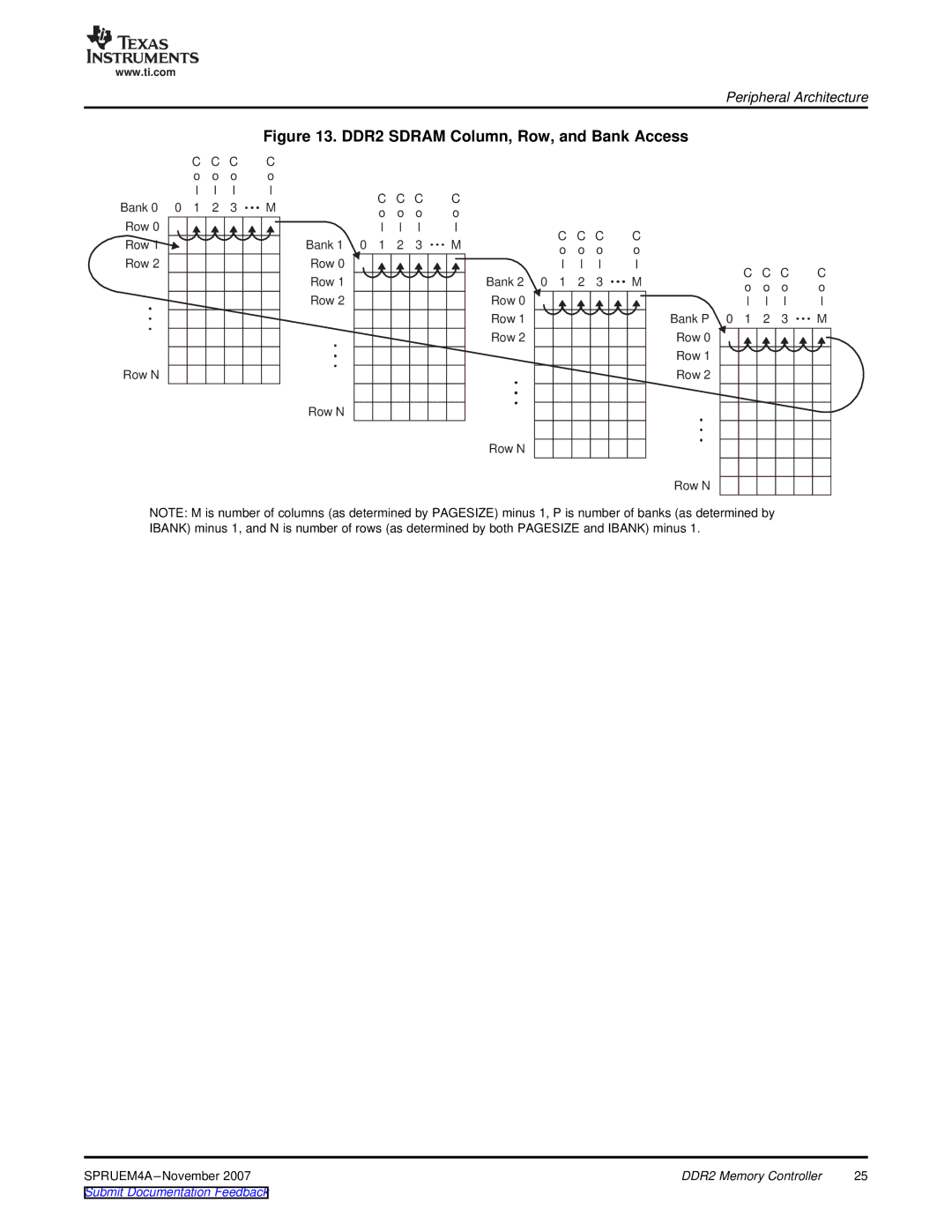
Figure 13. DDR2 SDRAM Column, Row, and Bank Access
|
| C | C C | C | |
|
| o | o | o | o |
|
| l | l | l | l |
Bank 0 | 0 | 1 | 2 | 3 | M |
Row 0 |
|
|
|
|
|
Row 1 |
|
|
|
|
|
Row 2 |
|
|
|
|
|
Row N |
|
|
|
|
|
|
| C C C | C | ||
|
| o | o | o | o |
|
| l | l | l | l |
Bank 1 | 0 | 1 | 2 | 3 | M |
Row 0 |
|
|
|
|
|
Row 1 |
|
|
|
|
|
Row 2 |
|
|
|
|
|
Row N |
|
|
|
|
|
|
| C | C C | C | |
|
| o | o | o | o |
|
| l | l | l | l |
Bank 2 | 0 | 1 | 2 | 3 | M |
Row 0 |
|
|
|
|
|
Row 1 |
|
|
|
|
|
Row 2 |
|
|
|
|
|
Row N |
|
|
|
|
|
|
| C C C | C | ||
|
| o | o | o | o |
|
| l | l | l | l |
Bank P | 0 | 1 | 2 | 3 | M |
Row 0 |
|
|
|
|
|
Row 1 |
|
|
|
|
|
Row 2 |
|
|
|
|
|
Row N |
|
|
|
|
|
NOTE: M is number of columns (as determined by PAGESIZE) minus 1, P is number of banks (as determined by IBANK) minus 1, and N is number of rows (as determined by both PAGESIZE and IBANK) minus 1.
DDR2 Memory Controller | 25 | |
Submit Documentation Feedback |
|
|
