www.ti.comArchitecture
|
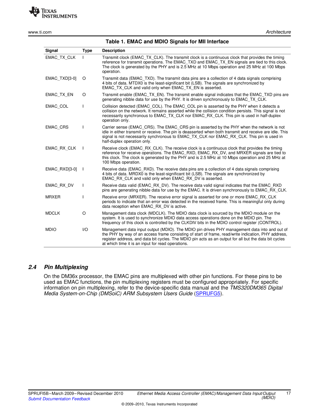
| Table 1. EMAC and MDIO Signals for MII Interface |
|
|
|
Signal | Type | Description |
|
|
|
EMAC_TX_CLK | I | Transmit clock (EMAC_TX_CLK). The transmit clock is a continuous clock that provides the timing |
|
| reference for transmit operations. The EMAC_TXD and EMAC_TX_EN signals are tied to this clock. |
|
| The clock is generated by the PHY and is 2.5 MHz at 10 Mbps operation and 25 MHz at 100 Mbps |
|
| operation. |
O | Transmit data (EMAC_TXD). The transmit data pins are a collection of 4 data signals comprising | |
|
| 4 bits of data. MTDX0 is the |
|
| EMAC_TX_CLK and valid only when EMAC_TX_EN is asserted. |
EMAC_TX_EN | O | Transmit enable (EMAC_TX_EN). The transmit enable signal indicates that the EMAC_TXD pins are |
|
| generating nibble data for use by the PHY. It is driven synchronously to EMAC_TX_CLK. |
EMAC_COL | I | Collision detected (EMAC_COL). The EMAC_COL pin is asserted by the PHY when it detects a |
|
| collision on the network. It remains asserted while the collision condition persists. This signal is not |
|
| necessarily synchronous to EMAC_TX_CLK nor EMAC_RX_CLK. This pin is used in |
|
| operation only. |
EMAC_CRS | I | Carrier sense (EMAC_CRS). The EMAC_CRS pin is asserted by the PHY when the network is not |
|
| idle in either transmit or receive. The pin is deasserted when both transmit and receive are idle. This |
|
| signal is not necessarily synchronous to EMAC_TX_CLK nor EMAC_RX_CLK. This pin is used in |
|
| |
EMAC_RX_CLK | I | Receive clock (EMAC_RX_CLK). The receive clock is a continuous clock that provides the timing |
|
| reference for receive operations. The EMAC_RXD, EMAC_RX_DV, and MRXER signals are tied to |
|
| this clock. The clock is generated by the PHY and is 2.5 MHz at 10 Mbps operation and 25 MHz at |
|
| 100 Mbps operation. |
I | Receive data (EMAC_RXD). The receive data pins are a collection of 4 data signals comprising | |
|
| 4 bits of data. MRDX0 is the |
|
| EMAC_RX_CLK and valid only when EMAC_RX_DV is asserted. |
EMAC_RX_DV | I | Receive data valid (EMAC_RX_DV). The receive data valid signal indicates that the EMAC_RXD |
|
| pins are generating nibble data for use by the EMAC. It is driven synchronously to EMAC_RX_CLK. |
MRXER | I | Receive error (MRXER). The receive error signal is asserted for one or more EMAC_RX_CLK |
|
| periods to indicate that an error was detected in the received frame. This is meaningful only during |
|
| data reception when EMAC_RX_DV is active. |
MDCLK | O | Management data clock (MDCLK). The MDIO data clock is sourced by the MDIO module on the |
|
| system. It is used to synchronize MDIO data access operations done on the MDIO pin. The |
|
| frequency of this clock is controlled by the CLKDIV bits in the MDIO control register (CONTROL). |
MDIO | I/O | Management data input output (MDIO). The MDIO pin drives PHY management data into and out of |
|
| the PHY by way of an access frame consisting of start of frame, read/write indication, PHY address, |
|
| register address, and data bit cycles. The MDIO pin acts as an output for all but the data bit cycles |
|
| at which time it is an input for read operations. |
|
|
|
2.4Pin Multiplexing
On the DM36x processor, the EMAC pins are multiplexed with other pin functions. For these pins to be used as EMAC functions, the pin multiplexing registers must be configured appropriately. For specific information on pin multiplexing, refer to the
SPRUFI5B
Submit Documentation Feedback | (MDIO) |
|
©