TVP5147M1PFP specifications
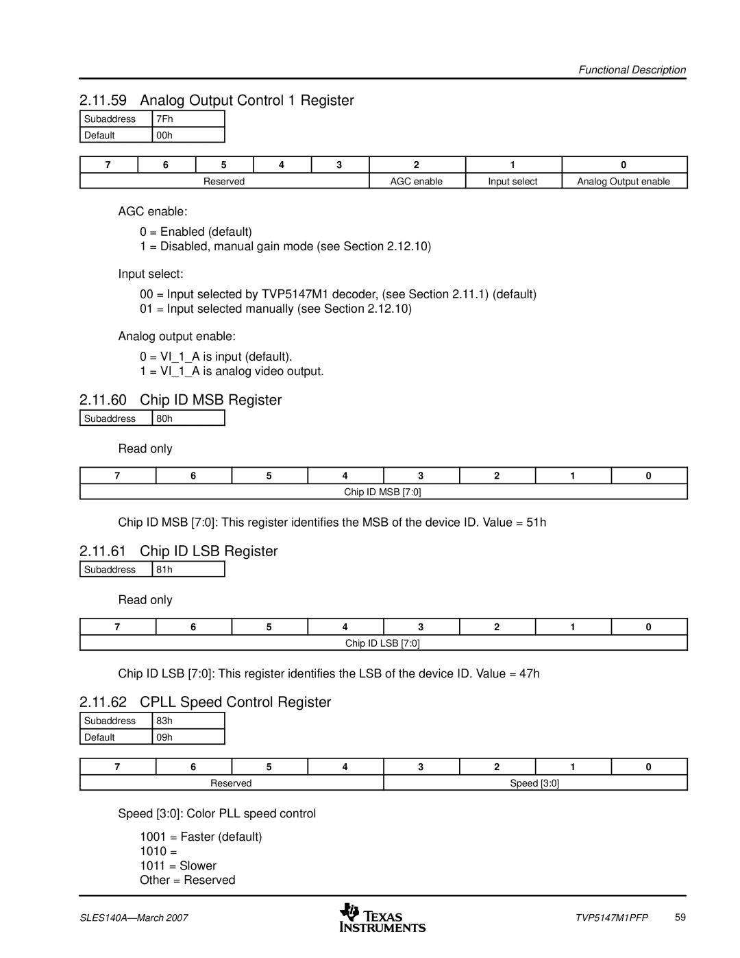
The Texas Instruments TVP5147M1PFP is a versatile video decoder that stands out in the realm of analog video processing. This device is particularly designed for high-quality video applications, making it an excellent choice for a variety of consumer and professional electronics that require reliable video decoding capabilities.One of the main features of the TVP5147 is its ability to decode multiple video formats, including NTSC, PAL, and SECAM. This flexibility allows the decoder to seamlessly interface with various video sources from different geographic regions, providing a global solution for video applications. The TVP5147 includes advanced synchronization features, ensuring it can effectively handle video signals that may vary in timing and quality.
The device is equipped with a sophisticated 10-bit analog-to-digital converter (ADC), which enhances the precision and clarity of the digital video output. This high-resolution capability allows for improved color accuracy and detail, leading to a more lifelike video representation. Additionally, the TVP5147 utilizes advanced digital processing technologies, including noise reduction and image enhancement features, contributing to outstanding image quality even in less than ideal input conditions.
Another notable characteristic of the TVP5147M1PFP is its support for various output formats, including ITU-R BT.601 and 656, which facilitates easy integration into different systems. The device can also provide various output resolutions, catering to the needs of diverse applications ranging from standard definition to high definition displays.
In terms of connectivity, the TVP5147 offers multiple input options, including composite video, S-video, and component video interfaces. This versatility ensures that it can accommodate a wide range of video sources, from traditional VHS players to modern digital cameras. Furthermore, the integrated video control features allow for easy adjustment of parameters such as brightness, contrast, and saturation.
The power consumption of the TVP5147M1PFP is optimized for low-energy applications while maintaining high performance, making it suitable for battery-powered devices and energy-efficient designs. Overall, the Texas Instruments TVP5147M1PFP is an exceptional video decoder that blends flexibility, high quality, and advanced technology, making it a preferred choice for video processing in numerous consumer and industrial applications. Its combination of features ensures reliable performance and high-quality output, fulfilling the demands of modern multimedia environments.

