CIRCUIT DESCRIPTION
frequency is low, the
The loop filter is formed by
4.3 RECEIVER CIRCUIT DESCRIPTION
NOTE: A block diagram of the RF and logic units is located on page
4.3.1 RF AMPLIFIER (Q1), FIRST MIXER (Q2)
The receive signal from the antenna is fed through
The signal is then fed to RF amplifier Q1. Imped- ance matching with FI1 is provided by L32, C4, C138, and R104. The RF amplifier is used to recover filter losses and improve the sensitivity of the receiver. The output of Q1 is fed to FI2 which is a bandpass filter similar to FI1. Impedance matching is provided by L5 and C7.
From FI2 the signal is fed to gate 1 of first mixer Q2. This is a
Impedance matching on the input of Q2 is provided by C11,
ance matching on the output is provided by C15, L9, L10, C18, C19, and R99. The first IF signal is then fed to
44.775 MHz | 1 | Mixer | 16 | |
2nd Injection |
| 44.775 |
|
|
| 2 | MHz |
| 15 |
Ceramic Filters | 3 | Oscillator | 45.225 | 14 |
| 450 kHz 2nd IF | |||
| MHz | |||
FI4, FI5, |
|
| ||
| 1st IF | 13 | ||
FI6 | 4 |
| ||
| Noise Det | |||
|
|
|
| |
| 5 |
| RSSI | 12 |
|
|
|
| |
| 6 |
| IF | 11 |
|
|
| Out | 10 |
| 7 |
| Quad. | |
|
| Detector | 9 | |
| 8 |
| Audio | |
|
| Amp | Out |
|
|
|
|
| |
Figure |
| Limiter/Mixer/Detector IC3 |
| |
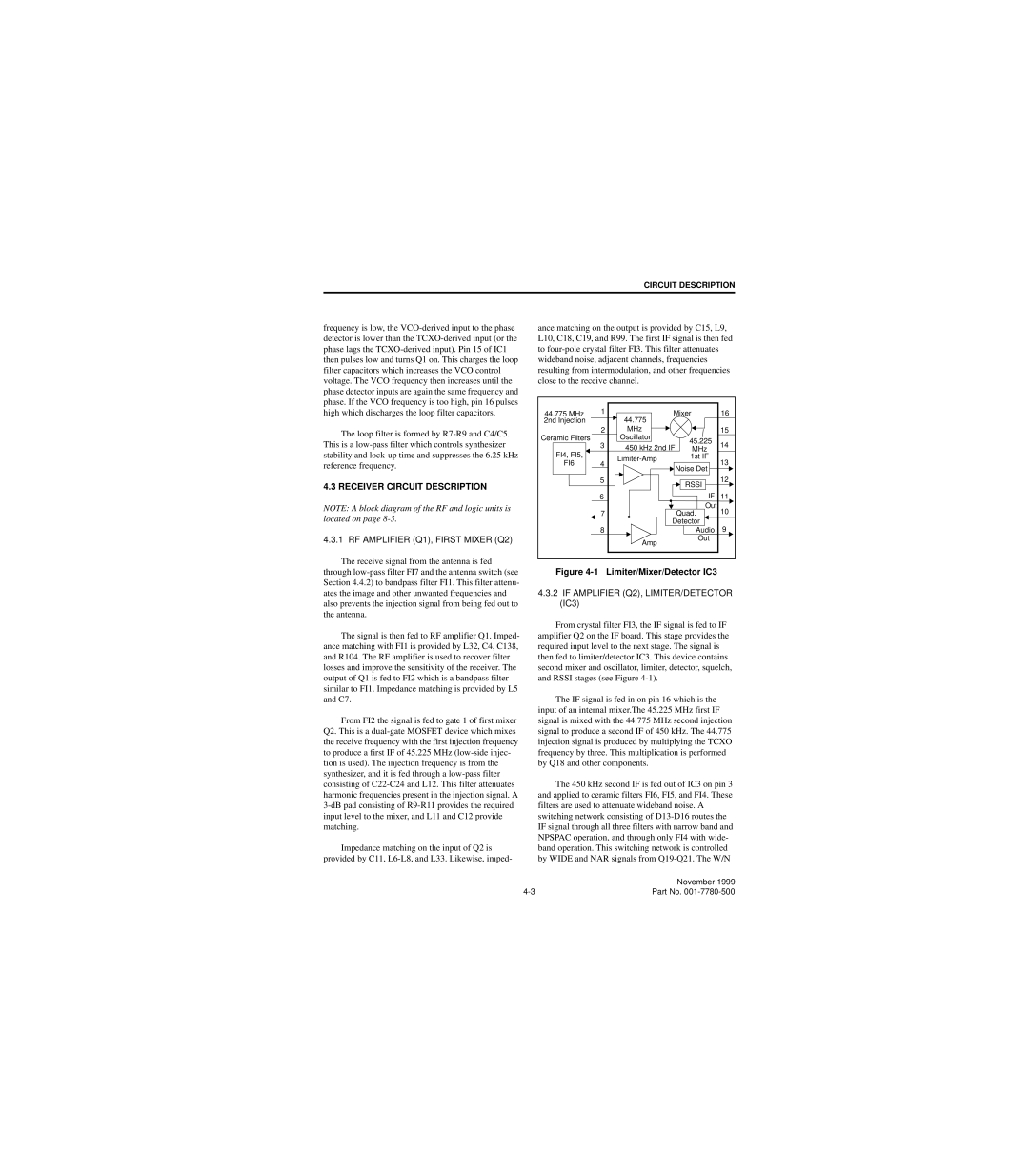
4.3.2IF AMPLIFIER (Q2), LIMITER/DETECTOR (IC3)
From crystal filter FI3, the IF signal is fed to IF amplifier Q2 on the IF board. This stage provides the required input level to the next stage. The signal is then fed to limiter/detector IC3. This device contains second mixer and oscillator, limiter, detector, squelch, and RSSI stages (see Figure
The IF signal is fed in on pin 16 which is the input of an internal mixer.The 45.225 MHz first IF signal is mixed with the 44.775 MHz second injection signal to produce a second IF of 450 kHz. The 44.775 injection signal is produced by multiplying the TCXO frequency by three. This multiplication is performed by Q18 and other components.
The 450 kHz second IF is fed out of IC3 on pin 3 and applied to ceramic filters FI6, FI5, and FI4. These filters are used to attenuate wideband noise. A switching network consisting of
| November 1999 |
Part No. |