EPSON
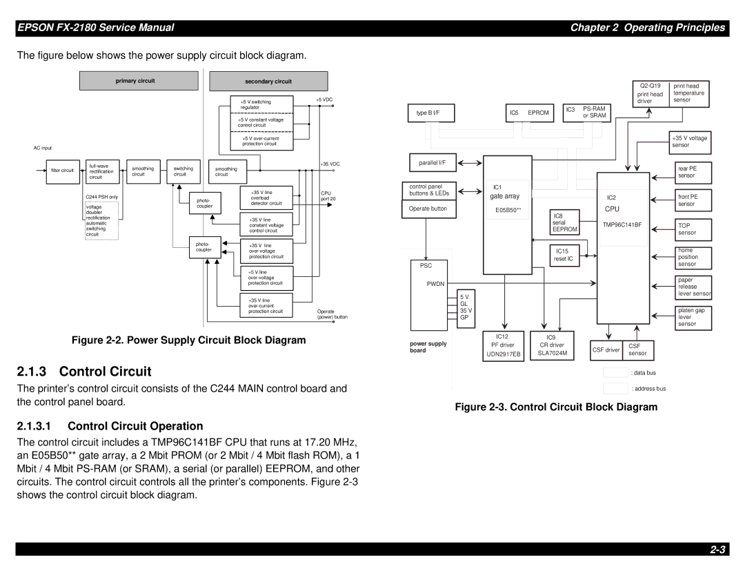
The figure below shows the power supply circuit block diagram.
primary circuit | secondary circuit |
Chapter 2 Operating Principles
AC input
filter circuit |
|
| smoothing |
| switching | |
| rectification |
|
| |||
|
| circuit |
| circuit | ||
|
| circuit |
|
| ||
|
|
|
|
|
|
C244 PSH only
photo-
voltagecoupler doubler
rectification automatic switching circuit
photo- coupler
+5 V switching | +5 VDC |
| |
regulator |
|
|
+5 V constant voltage control circuit
+5 V
smoothing | +35 VDC |
| |
circuit |
|
+35 V line | CPU |
overload | port 20 |
detector circuit |
|
+35 V line |
|
constant voltage |
|
control circuit |
|
+35 V line |
|
| |
protection circuit |
|
+5 V line |
|
| |
protection circuit |
|
+35 V line |
|
| |
protection circuit | Operate |
| (power) button |
print head | |
print head | temperature |
driver | sensor |
type B I/F |
| IC5 | EPROM |
| IC3 | |||
|
| or SRAM | ||||||
|
|
|
|
|
|
| ||
|
|
|
|
|
|
|
|
|
|
|
|
|
|
|
|
|
|
|
|
|
| +35 V voltage |
|
|
|
| sensor |
parallel I/F |
|
|
| rear PE |
|
|
|
| |
|
|
|
| sensor |
control panel | IC1 |
|
|
|
buttons & LEDs | gate array |
| IC2 | front PE |
|
| |||
Operate button | E05B50** |
| CPU | sensor |
IC8 |
| |||
|
|
|
| |
|
| serial | TMP96C141BF | TOP |
|
| EEPROM | ||
|
|
| sensor | |
|
|
|
| |
|
| IC15 |
| home |
|
| reset IC |
| position |
|
|
| sensor | |
PSC |
|
|
| |
|
|
|
| |
PWDN |
|
|
| paper |
|
|
| release | |
|
|
|
| |
| 5 V |
|
| lever sensor |
|
|
|
| |
| GL |
|
| platen gap |
| 35 V |
|
| |
| GP |
|
| lever |
|
|
|
| sensor |
Figure 2-2. Power Supply Circuit Block Diagram
2.1.3 Control Circuit
The printer’s control circuit consists of the C244 MAIN control board and the control panel board.
2.1.3.1Control Circuit Operation
The control circuit includes a TMP96C141BF CPU that runs at 17.20 MHz, an E05B50** gate array, a 2 Mbit PROM (or 2 Mbit / 4 Mbit flash ROM), a 1 Mbit / 4 Mbit
power supply | IC12 |
| IC9 |
|
|
|
|
|
|
|
PF driver |
| CR driver |
| CSF driver |
| CSF |
| |||
board | UDN2917EB |
| SLA7024M |
|
| sensor |
| |||
|
|
|
|
|
|
| ||||
|
|
|
|
|
|
|
|
|
|
|
|
|
|
|
|
|
|
| : data bus | ||
|
|
|
|
|
|
|
| |||
|
|
|
|
|
|
|
| : address bus | ||
|
|
|
|
|
|
|
| |||
|
|
|
|
|
|
|
|
|
|
|