Table of Contents
Introduction
Software Security
Separate ADDRESS/DATA BUS
Module Description ON±BOARD Memory Package
Large Nonvolatile Memory
IN±SYSTEM Loading
High Reliability Operation
DS2250T Soft Microcontroller Module
Product Description
DS5000FP Soft Microprocessor Chip
DS5000T Soft Microcontroller Module
DS2251T 128K Soft Microcontroller Module
DS5002FP Secure Microprocessor Chip
DS2252T Secure Microcontroller Module
Speed Clock Part Number
Selection Guide
Chip Description Maximum Speed Part Number
Module Description
Secure Microcontroller Architecture
Secure Microcontroller Architectural Block Diagram Figure
High±Reliability Circuitry
Timed Access Logic
Parallel I/O
Program/Data RAM Interface
Resident Loader ROM
Watchdog Timer
Internal Registers
Programmers Guide
Secure Microcontroller Memory Organization
Secure Microcontroller Memory MAP ±1
Scratchpad Register MAP ±2
Program and Data Memory
PSW.4±3 R1±R0 Register Bank Select
Bank Starting Address R0
Important Application Note
DS5000 Series Memory Organization
DS5000 Series Memory MAP ±3
Memory map. The first is the EA pin. The second is
Overrides the condition of the EA pin as well
DS5000 Memory Map Control
DS5000 Series Mcon Register ±4 Bit Description
PA3
MCON.2 ECE2
DS5001/DS5002 Memory Organization
MCON.3
RA32/8
PA3 PA2 PA1 PA0 Partition BYTE±WIDE BUS Memory MAP
RG1 RG0 Range CE1 Access CE2 Access
CE1 CE2 CE3
Msel RG1 RG0 Program Data Program Access Data Access
Partitionable Memory MAP for DS5001/DS5002 Series ±5
CE1 CE3 CE4
DS5001/DS5002 Memory Mapped Peripherals
NON±PARTITIONABLE Memory MAP for DS5001, DS5002 Series ±6
DS5001/DS5002 Memory Map Control
Peripheral Enables in the Data Memory MAP ±7
MCON.2 PES
DS5001/DS5002 Series Mcon Register ±8
PA3 PA2 PA1 PA0 RG1 PES
MCON.3 RG1
RPCTL.0 RG0
Loading and Reloading Program Memory
RPCTL.5 Exbs
RPCTL.4
050396 23/173
Reloading Portions of a DS5000 Series Device ±10
Soft Reload of a DS5001/DS5002
Reloading a DS5001/DS5002 Series Device ±11
Special Function Registers
ECE2
DS5000 Series Special Function Register MAP ±12
CRC
DS5001/DS5002 Series Special Function Register MAP ±13
Label Pcon Register Address 087H
Power Control Register
PCON.0 IDL
PCON.3EPFW
PCON.2 EWT
PCON.1 Stop
Label Tcon Register Address 088H
Timer Control Register
Gate
Timer Mode Register
Label Tmod Register Address 089H
TCON.0 IT0
LabelSCON Register Address 098H
Serial Control Register
ET1
Interrupt Enable Register
LabelIE Register Address 0A8H
SCON.0
LabelIP Register Address 0B8H
Interrupt Priority Register
CRC.1 MDM
DS5001 CRC Register
Label CRC Register Address 0C1H
RNGE3±0
RA32/8
DS5000 Memory Control Register
LabelMCON Register Address 0C6H
PA3 PA2 PA1 PA0
DS5001 Mcon Register
Label Mcon Register Address 0C6H
MCON.0
Accessed by Movx instructions on the Byte±wide bus
LabelPSW Register Address 0D0H
Program Status Word Register
RPCTL.3 IBI
DS5001/DS5002 RPC Control Register
Label Rpctl Register Address 0D8H
RPCTL.7 RNR
IA0
DS5001/DS5002 RPC Status Register
Label RPS Register Address 0DAH
RPCTL.1 Rpcon
OBF
RPS.1
IBF
RPS.0
Setb 00H
Instruction SET
Addressing Modes
ADD A, R4
Address
±20 Branch to the location PC+2 ±
Addressing
Acall 100H Call to the subroutine at
Instructions That Affect Flag Settings
Program Status Flags
Flags Instruction OV AC
25C 40C 70C
Memory Interconnect
Recommended SRAMs for USE with Soft Microcontrollers ±1
Data Reten Part Tion Current RAM Size Vendor
Memory Interconnect of the DS5000FP ±1
DS5000 Series Module Block Diagram ±2
Memory Interconnect of the Partitionable DS5001/DS5002 ±3
Óóóóóóóóó Ó
Óóóóóóóó 52 14Ó GND
Memory Interconnect Using the 128K Sram ±5
DS2251T±128 Block Diagram ±6
Ôôôôôô
DS2252T±32 Block Diagram ±7
LITHIUM/BATTERY Backup
Battery Backed Circuits
Data Retention
Battery attached
Power Supply Slew Rate ±1
Battery Attach Procedure
Battery Lifetime
54 * 10±3
180 * 10±3
2400 + 75 * 10±9 * 24 21.68 * 10±3
Freshness Seal
Lithium Battery Usage
ªPower On Resetº
Power Management
Idle Mode
CONTROL/STATUS Bits for Power Control ±1 Bit Description
PCON.3 Epfw
Stop Mode
Mode Program ALE Psen Memory
PIN States in IDLE/STOP Modes ±1
Voltage Monitoring Circuitry
Secure Microcontroller Power Cycling Timing ±2
Vpfw threshold is above the specified minimum
Power Fail Interrupt
Total Power Failure
Partial Power Failures
Reset Vector
Secure Microcontroller Power Management ±3
Timed Access
Timed Access ±1
Software Control
BIT Name Micro Version Location Description
Timed Access Protected Control Bits ±1
050396 66/173
Watchdog Timer ±2
0C7H, #055H 2nd TA Value
IP.7
CRC Memory Verification
Watchdog Timer Control Bits
CRC.0
DS5001 CRC Register Address 0C1h
Range 3±0
CRC.1
This routine tests the CRC±16 circuit in the DS5001FP
CRC Code Example ±3
DS5001 DS5000 DS5002
Feature
Firmware Security
Security Overview
Security Lock
RAM Memory
Encrypted Memory
DS5002 Software Encryption Block Diagram ±2
DS5000 Software Encryption Block Diagram ±1
050396 74/173
Encryption Algorithm
Encryption Key
Encryption Key Selection and Loading
Dummy BUS Access Timing ±3
Dummy Bus Access
Random Number Generator
On±chip Vector RAM
Self±Destruct Input
Microprobe/Die Top Coating
Security Summary by Part
DS5000FP / DS5000T / DS2250T
DS5001FP / DS2251T
Application Advanced Security Techniques
Change Code
External Circuits
Tamper Protection
Reset Conditions
Reset Sources
Reset Status Bits ±1
Special Function Register Reset States ±1
Reset Condition Reset Type
Register
Power On Reset
Power on Reset Timing ±2
Chanical and some time is required to get the mass
No±VLI Power On Reset
External Reset
Watchdog Timer Reset
Application Reset Routine Example
Memory Interrupts TIMERS/SERIAL Protection
Memory Map
Timed ± DS5000 only
Interrupts
Protection
Timers
Tively. Shown here is an example of Timer and Serial
Microprocessor disables timer activity excluding
Interrupt Source Vector Address Flag Flag Location
Interrupt Source Enable BIT Location
Interrupts
Interrupt Sources
External Interrupts
Timer Interrupts
Power±fail Warning Interrupt
Machine cycle when the interrupts are enabled. INT0 is
Interrupt Request Sources ±1
Simulated Interrupts
Interrupt Enable Control Bits ±2 Bit Description
ET0
EX0
IP.4
Interrupt Priorities
Interrupt Priority Control Bits ±3 Bit Description
Priority Flag Interrupt Source
Interrupt Acknowledge
Interrupt Acknowledge Sequence ±4
Flag Vector Address Interrupt Source
050396 94/173
Function
Parallel I/O Overview
Port 0 Functional Circuitry ±1
PIN Name
Port 2 Functional Circuitry
Port 1 Functional Circuitry
Output Functions
Port 3 Functional Circuitry
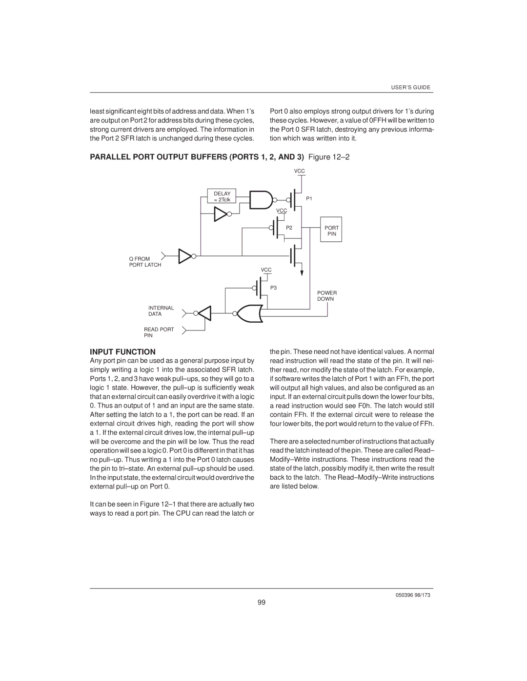
Input Function
Parallel Port Output Buffers Ports 1, 2, and 3 ±2
Port 0 D0±7
READ±MODIFY±WRITE Instructions
Reprogrammable Peripheral Controller RPC
Mnemonic Description
RPC Interrupts
USE of the RPC Mode ±3
USE of the RPC Mode ±4
Command
ST7 ST6 ST5 ST4 IAO IBF OBF
RPC Status Register ± Status Address 0DAH ±5
103
RPC Protocol
DMA Operation
Dbbout
Rpcon bit is set
Port 2 becomes the control signals as shown in ±3
RPC Control Register ± Rpctl Address 0D8H ±6
RNR Exbs IBI DMA Rpcon RG0
Programmable Timers Functional Description
TMOD.6 Timer TMOD.2 Timer
Tmod Register Control BIT Summary ±1 Bit Description
Tcon Register CONTROL/STATUS Bits ±2
TMOD.5, TMOD.4
TMOD.1, TMOD.0
107
TIMER/COUNTER Mode 0 and 1 Operation ±3
Mode
Scribed for TR0, TF0, and INT0
108
TIMER/COUNTER Mode 2 Operation ±4
109
Timer 0 Mode 3 Operation ±5
START/STOP
Mode SYNC/ASYNC Baud Clock
Serial I/O Function Description
Serial Port Operating Modes ±1
ªXmit Bit 8º
Mode Function Word Length Period
Mode Sync Bits CLK Async Timer 1 Overflow
Serial Port Control Register ±1 Bit Description
Baud Rate Generation
SCON.2 RB8
SCON.1
SCON.0
Baud Rate BPS
Timer 1 Baud Rate Generation ±2
Synchronous Operation Mode
Smod Timer TH1
114
115
Mode 0 Block Diagram and Timing ±2
116
Asynchronous Operation
Mode 2
Smod BRG Clock
117
118
Serial Port Mode 1 Block Diagram ±3
119
MODE2 and 3 Block Diagram ±4
Mode Function Word Length Baud Clock
Application Serial Port Initialization
Serial I/O Operating Modes
PT1 PX1 PT0 PX0
SM0 SM1 SM2 REN
TB8 RB8
ET1 EX1 ET0 EX0
Smod POR PFW WTR Epfw EWT Stop IDL
TF1 TR1 TF0 TR0
IE1 IT1 IE0
123
XTAL1
CPU Timing Oscillator
Crystal Connection ±1
Clock Source Input ±2
125
Instruction Timing
BYTE±WIDE RAM Instruction Execution Timing ±3
Expanded Program Memory Timing
126
127
Expanded Program Memory Fetch ±4
Expanded Data Memory Read ±5
Expanded Data Memory Write ±6
128
Expanded Data Memory Timing
Complete RD cycle, including activation of ALE and RD
129
130
Invoking the Bootstrap Loader
Program Loading Introduction
DS5000FP DS5001/2FP
131
DS5000 Series
DS5001/DS5002 Series
Exiting the Loader
MODEM=1 PROG=0
132
Serial Program Load Mode
Serial Load Configuration ±2
133
57600
AUTO±BAUD Rate Detection
Baud Rate
Crystal Freq MHz 300 1200 2400
Command Function Version
Bootstrap Loader Initialization
Command Line Interface
Command Line Syntax
ABC → 0ABCH Abcd → 0ABCDH Abcde → 0BCDEH
Command Summaries
Begin±address end±address
→ 000AH AB → 00ABH
P0 value P1 value P2 value P3 value
Byte begin±address end±address
Byte±1 byte±2 byte±3 byte±4 byte±5
Byte
MSL
Xon/Xoff
CRC/MCON/MSL/RPCTL byte
Mcon
Eillopt
Error Messages Eargreq
Eextarg
Eillcmd
140
Intel HEX File Format
141
Parallel Program Load Configuration ±3
Parallel Program Load Operation
Parallel Program Load Cycles ±4
P2.7 P2.6 P2.5
Parallel Program Load Mode
Mode RST Psen Prog
8751±COMPATIBLE Program Load Cycles ±3
143
RPC Program Mode Operation
Parallel Programming Concerns
Pulses specified, each with a low time of 90 to
144
DS5000T/DS2250T Functional Block Diagram ±1
REAL±TIME Clock
DS1215 Phantom Time Chip
145
146
Pattern Comparison Register Description ±2
147
DS1215 Register Entry Flowchart ±3
148
DS1215 Time Registers Description ±4
Registers
Special Bits
149
Time Register Examples ±5
150
DS1283 Watchdog Timekeeper Chip
DS2251T/DS2252T RTC Block Diagram ±6
Memory MAP
151
152
DS1283 REAL±TIME Clock Memory MAP ±7
DS1283 REAL±TIME Clock Command Register ±8
Mask
Alarm Maskbit Operation ±9
Alarm Condition
DS1283 RTC Interrupts
155
Application Using the DS5000T RTC DS1215 Example
156
Wbyte
157
RET
158
159
Application Using the DS2251T RTC DS1283 Example
160
161
162
163
Time Microcontroller Reads the Wrong Time
Troubleshooting
Unexplained Device Resets
RAM Loses Data When Powered Down
Unable to Invoke Stop Mode
Serial Port does not Work
Program will not Execute
DS5000TK KIT does not Respond to KIT5K Software
High Current Drain in Stop Mode
Data is Lost or Corrupted
INT0 is Stuck LOW on DS2252T
DOS
Mnemonic Instruction Code HEX Byte Cycle Explanation
Instruction SET Details
CLR a CPL a
DA a
RRC a
RL a
RLC a
RR a
Mnemonic Instruction Code HEX Byte
ANL C, bit = C and bit
CLR bit Bit =
Setb bit Bit =
CPL bit Bit = bit
RET
Reti
Dptr
NOP