Installation and Use
Page
Safety Summary
Flammability
CE Notice European Community
Limited and Restricted Rights Legend
Contents
Chapter
Connector Pin Assignments
Appendix a
Appendix D Related Documentation
Page
List of Figures
Page
List of Tables
Xvi
Model Number Description
About This Manual
Summary of Changes
Overview of Contents
Comments and Suggestions
Bold
Conventions Used in This Manual
Introduction
Hardware Preparation and Installation
MVME2603/2604 Base Board Block Diagram
Overview of Startup Procedure
Equipment Required
Startup Overview
What you need to do Refer to
Connector Pin Assignments
Unpacking Instructions
Hardware Configuration
MVME2603/2604 Base Board Preparation
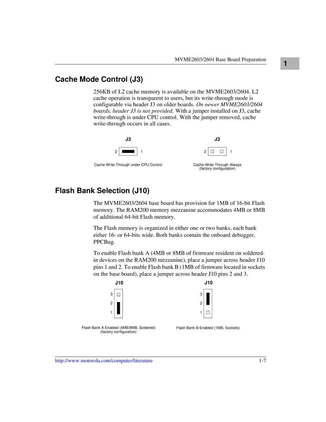
Flash Bank Selection J10
Cache Mode Control J3
Serial Port 4 Receive Clock Configuration J16
MVME2603/2604 Switches, Headers, Connectors, Fuses, LEDs
Serial Port 4 Transmit Clock Configuration J17
Serial Port 4 Transmit Clock Receiver Buffer Control J20
Serial Port 3 Transmit Clock Configuration J18
System Controller Selection J22
Remote Status and Control
MVME712M Transition Module Preparation
MVME712M Transition Module Preparation
Literature1-16Computer GroupCenter
OnnectorCLocationsFigure 1-3. MVME712Mand Header
MVME712M Port/Jumper Correspondence
Serial Ports 1-4 DCE/DTE Configuration
Serial Port 4 Clock Configuration
Serial Port Board Panel Connector Jumper Header
MVME712M Serial Port 1 DCE/DTE Configuration
MVME712M Serial Port 2 DCE/DTE Configuration
MVME712M Serial Port 3 DCE Configuration
MVME712M Serial Port 3 DTE Configuration
MVME712M Serial Port 4 DCE Configuration
10. MVME712M Serial Port 4 DTE Configuration
P2 Adapter Preparation
11. MVME712M P2 Adapter Component Placement
MVME761 Transition Module Preparation
12. MVME761 Connector and Header Locations
Synchronous Board
Configuration of Serial Ports 3
Port Connector Header J12
Serial Ports 1
J2J2
13. MVME761 Serial Ports 1 and 2 DCE Only
14. MVME761 Serial Ports 3 and 4 DCE Configuration
15. MVME761 Serial Ports 3 and 4 DTE Configuration
P2 Adapter Preparation Three-Row
P2 Adapter Preparation Five-Row
16. MVME761 P2 Adapter Three-Row Component Placement
17. MVME761 P2 Adapter Five-Row Component Placement
RAM200 Memory Mezzanine Installation
Hardware Installation
Hardware Preparation and Installation
18. RAM200 Placement on MVME2603/2604
PMC Module Installation
Hardware Preparation and Installation
19. PMC Module Placement on MVME2603/2604
PMC Carrier Board Installation
20. PMC Carrier Board Placement on MVME2603/2604
MVME2603/2604 VME Module Installation
Hardware Installation
MVME712M Transition Module Installation
Hardware Installation
Hardware Preparation and Installation
21. MVME712M/MVME2603/2604 Cable Connections
MVME761 Transition Module Installation
22. MVME761/MVME2603/2604 Cable Connections
System Considerations
MVME2603/2604 VME Module
Hardware Preparation and Installation
System Considerations
Page
Operating Instructions
Applying Power
PPCBug System Startup
Abort Switch S1
Reset Switch S2
Applying Power
Front Panel Indicators DS1 DS6
Processor Memory Map
Memory Maps
Default Processor Memory Map
Processor Default View of the Memory Map
Processor Address Size Definition Start End
VMEbus Memory Map
PCI Local Bus Memory Map
Programming Considerations
VMEbus Master Mapping
PCI Arbitration
PCI Arbitration Assignments
PCI Bus Request PCI Masters
Programming Considerations
Interrupt Handling
MVME2603/MVME2604 Interrupt Architecture
Controller DMA Assignment Priority Label
Sources of Reset
DMA Channels
IBC DMA Channel Assignments
Asic
Classes of Reset and Effectiveness
Endian Issues
Processor/Memory Domain
PCI Domain
VMEbus Domain
PCI and Scsi
ECC Dram
Features
MVME2603/2604 Features
Feature Description
Scsi I/O
VME I/O
General Description
MVME2603/2604 Block Diagram
Block Diagram
Scsi Termination
Scsi Interface
Ethernet Interface
Mezzanine Type
PMC Connectors
Signaling Voltage
PCI Mezzanine Interface
ISA Super I/O Device Isasio
VMEbus Interface
Parallel Port
Asynchronous Serial Ports
PCI-ISA Bridge PIB Controller
Disk Drive Controller
Keyboard and Mouse Interface
Real-Time Clock/NVRAM/Timer Function
Interval Timers
Programmable Timers
Serial Communications Interface
Bit Timers
SD7 SD6 SD5 SD4 SD3 SD2 SD1 SD0
Base Module Feature Register
Base Module Feature Register Offset $0802
Z8536 CIO Device
P2 Multiplexing Sequence
P2 Signal Multiplexing
RI2
RLB4 DCD4 Idreq ∗ TM4/MID2 DTR1 RI4 DTR2 RI1
DSR1
DCD1
Front Panel Indicators DS1 DS6
Fuse Voltage
Polyswitches Resettable Fuses
Power
Fuse Assignments
PM603/604 Processor
Speaker Control
Flash Memory
RAM200 Memory Module
MVME712M Transition Module
Serial Interface Modules
MVME761 Transition Module
Model Module Number Type
SIM Type Identification
Page
MVME2603/2604 Connectors
Connector Pin Assignments
Connector Pin Assignments
Common Connectors
LED Mezzanine Connector J1
LED Mezzanine Connector
GND
Debug Connector J2
Debug Connector
PA0 PA1
PDPAR6 PDPAR7
PDPAR0 PDPAR1
PDPAR2 PDPAR3
PDPAR4 PDPAR5
TT3 TC0
TT0 TSIZ0
TT1 TSIZ1
TT2 TSIZ2
Floppy/LED Connector
Floppy/LED Connector J4
PCI Expansion Connector
PCI Expansion Connector J5
PAR
Trst ∗ PMC2P ∗ PMC2GNT ∗ PMC2REQ ∗
Lock ∗ Sdone Devsel ∗
GND Trdy ∗ Irdy ∗
PAR64
Keyboard and Mouse Connectors J6, J8
Keyboard Connector
Mouse Connector
Dram Mezzanine Connector J7
Dram Mezzanine Connector
Aras ∗ Acas ∗
RDL60 RDL61
RDL6 RDL7 RDL8 RDL9 RDL10 RDL11 RDL12
RDL56 RDL57
RDL58 RDL59
RDU0 RDU1
CDL2 CDL3
CDL4 CDL5
CDL6 CDL7
PCI Mezzanine Card Connectors
PCI Mezzanine Card Connector
J11 J12
J13 J14
GND PMCIO18 PMCIO19
GND PMCIO12 PMCIO13
PMCIO14 PMCIO15
PMCIO16 PMCIO17
VMEbus Connector P1
VMEbus Connector P1
Row Z Row a Row B Row C Row D
VMEbus Connector P2
10. VMEbus Connector P2 MVME712M I/O Mode
MVME712M-Compatible Versions
PMCIO8 GND
PMCIO4 GND
PMCIO6 GND
SDBP0
Termpwr GND ATN ∗ BSY ∗ ACK ∗ RST ∗ MSG ∗ SEL ∗ REQ ∗
Scsi Connector
11. Scsi Connector MVME712M
GND DBP ∗
12. Serial Connections-MVME712M Ports
Serial Ports
GND Prbsy Prpe Prsel Inprime ∗
Parallel Connector
13. Parallel I/O Connector MVME712M
Prstb ∗ GND PRD0 PRD1 PRD2 PRD3 PRD4 PRD5 PRD6 PRD7
14. Ethernet AUI Connector MVME712M
Ethernet AUI Connector
15. VMEbus Connector P2 MVME761 I/O Mode
MVME761-Compatible Versions
PMCIO16
16. Serial Connections-Ports 1 and 2 MVME761
17. Serial Connections-Ports 3 and 4 MVME761
Serial Ports 3
18. Parallel I/O Connector MVME761
Prbsy GND Prsel
GND Prpe PRD0 PRD1 PRD2 PRD3 PRD4 PRD5 PRD6 PRD7
19. Ethernet 10BaseT/100BaseTX Connector MVME761
Ethernet 10BaseT/100BaseTX Connector
Page
Overview
PPCBug
PPCBug Implementation
Memory Requirements
Using the Debugger
Debugger Commands
Debugger Commands
Command Description
Forkwr
Gevboot
ENV
Fork
MD, MDS
Pboot
Reset
MAW
SYM
RUN
SET
Srom
Diagnostic Tests
Diagnostic Test Groups
Test Set Description Applicability
Cnfg and ENV Commands
Cnfg Configure Board Information Block
ENV Set Environment
Configuring the PPCBug Parameters
Remote Start Method Switch G/M/B/N = B?
Wide Scsi 16-bit bus Narrow Scsi 8-bit bus. Default
Nvram Bootlist GEV.fw-boot-path Boot Enable Y/N = N?
Default = $00
Auto Boot Abort Delay = 7?
ROM Boot Direct Ending Address = FFFFFFFC?
Default Starting Address is $00000000
ROM Next Access Length 0 15 = 0?
Configuring the VMEbus Interface
PCI Slave Image 0 Bound Address Register = 00000000?
PCI Slave Image 3 Control = C0400000?
VMEbus Slave Image 1 Base Address Register = 00000000?
VMEbus Slave Image 3 Translation Offset = 00000000?
Specifications
Table A-1. MVME2603/2604 Specifications
Characteristics Specifications
Cooling Requirements
FCC Compliance
Page
Synchronous Serial Ports
Asynchronous Serial Ports
EIA-232-D Connections
Pin Signal Signal Name and Description Number Mnemonic
Table B-1. EIA-232-D Interconnect Signals
BSY
Interface Characteristics
Table B-2. EIA-232-D Interface Transmitter Characteristics
Table B-3. EIA-232-D Interface Receiver Characteristics
EIA-530 Connections
Table B-4. MVME761 EIA-530 Interconnect Signals
EIA-530 Connections
Table B-5. EIA-530 Interface Transmitter Characteristics
Proper Grounding
Table B-6. EIA-530 Interface Receiver Characteristics
Page
Table C-1. Troubleshooting MVME2603/2604 Boards
CTroubleshooting CPU Boards Solving Startup Problems
Troubleshooting CPU Boards Solving Startup Problems
Introduction
Troubleshooting Procedure Complete
Document Title Publication Number
Motorola Computer Group Documents
Document Title and Source Publication Number
Manufacturers’ Documents
MPC2604GA
MPCFPE/AD
CA91C042
Related Specifications
ANSI/IEEE
IEC 821 BUS
Isbn
MPR-PPC-RPU-02
TIA/EIA-232
Member countries
Page
Index
Dram
Romnal Scsi
PCI bus 2-4,2-7,3-3,3-7,3-11,3-17
10,2-14,2-16,3-8,3-17 uppercase