Modem User’s Guide
3600
Motorola
Copyright
Updates
Trademarks
Regulatory Information
FCC Requirements
FCC Fax Branding Requirements
FCC Part 15 Declaration Of Conformity
Model Name V.3600, 115 VAC version only
Shielded Cables
Model Name V.3600, all other versions
Special Requirements For Canada
Industry Canada IC Requirements
Ringer Equivalence Number
Canadian Emission Requirements V.3600, other versions
Page
Contents
Contents
Contents
Test Mode Operation
Protocols
Security
Fax Operation
Status Registers
Contents
25 bis Autodialer
Maintenance
Appendix A. Specifications
Appendix D. Fault Isolation Procedure
Appendix B. Phone Jack Descriptions
Appendix E. Command Index and Defaults
Chapter Introduction
Shelf-Mount Units
Features
Data Mode
Fax Mode
Software
Communications Software Class 1 Fax Communications Software
Internet Browser
Functional
Description
Physical
Rear Panel 115 Vac Model
RM16M Unit
RM16M Version
Chapter Installation
Electrical Installation
AC Power Connection
DC Power Connection
Installation
DTE Connection
Digital Interface Signals
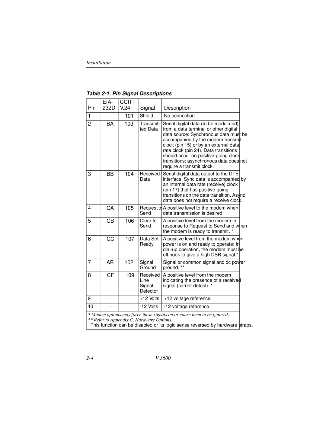
Pin Signal Descriptions
140
Dial Mode Pstn Connection Dial jack
Telephone Line Connection
Leased Line Connection TELSET/LEASED Line Jack
Direct connection to the Pstn is shown in Figure
Leased Line Connection 115 Vac Model
Shelf-Mount RM16M V.3600 Installation
RM16M Connections
Page
Chapter Getting Started
Power-Up
Option Selection
Autodialing from a Terminal with the AT Commands
Placing a Call
Dialing with a Standard Telephone
Autodialing from Front Panel
Answering a Call
Ending a Call
Reasons for Call Termination
Condition
Reasons for Call Termination
Page
Chapter Front Panel Operation
LED Descriptions
LCD Menus
LCD Menu Operation
Main Menu LCD Messages Reg
Main Menu Submenu Submenu Item Option Com Reg
Remote Initiate
Submenu Main Menu Option Com Reg
RATION? OPTIONS?
Lease line only † Dial line only 3600
Modify Change DTE Speed DTE=DCE
Modify Change DTE Dial Method Async
Modify Change DTE RTS/CTS Delay
Password of 0000 disables front panel security 3600
Front Panel Security
Page
Command Categories
Chapter AT Commands
Operation Modes
Offline Command Mode
Sending Commands to the Modem
Online Command Mode
Creating a Command Statement AT
Autobaud Guidelines for Creating Command Statements
Command Statement Buffer
Repeating a Command a
Monitor Display
Backspace Key
Numbered Commands
Response Commands
Group Commands
Digit / Word Selection
Response Displays Q
Negotiation Displays W
Connect Message Codes \V
Call Progress / Connect Speed Messages
Command Code Set Number Operation
Number Code Application *RC
Response Number Codes / Messages
Message Meaning
DTE rate 31200 bps
Connect 300/V42
Connect 300/MNP5
Dial Commands
Dialing D
Pulse Dialing P
Tone Dialing T
Insert Long Pause
Switching to Answer Mode after Dialing R
Remaining in Command Mode
Wait for Second Dial Tone W
Hook Flash
Wait for 5 Seconds of Silence @
Dialing a Stored Telephone Number Sn
Autodial Number Location *AUn
Voice Calls
Switching from Voice to Data
AT Command Answer a
Manual Answer
Autoanswer S0
Distinctive Ring *DR
Caller ID Messages Modem sends this message
Terminal Interface Commands
Data Carrier Detect &C
Data Set Ready &S
Data Terminal Ready &D
Serial Port Ring Indicator Pin 22 \R
Request to Send / Clear to Send &R
General Commands
Changing from Data Mode to Command Mode +++
DTE Controlled Fallback Rate Pin 23 *FB
Local Character Echo E
Hanging Up H, H1
Online Character Echo F
Fast Disconnect H2, H3
Eprom Check
Speaker Volume L
Speaker Control M
Asynchronous / Synchronous Mode Selection &M
Return Online O
Long Space Disconnect Y
Bis Guard Tones &G
Make / Break Dial Pulse Ratio &P
Comman Operation
Synchronous Transmit Clock Source &X
Rate Selection Thresholds *TH
Asymmetric Bit Rates *AS
Modulation *MM
Maximum DCE Speed %B
Minimum DCE Speed %L
Auto Retrain %E
Automatic Rate Adaption %R
Manual Rate Adaption *RR
Product Revision Level %V
Online Quick Reference $H
Product Serial Number $V
Talk / Data *DA
Fast Train *FT
Disable AT Command Set *NT
Wire Operation
Private Line Operation
Dial Line Transmit Level *TDn
Wire Leased Line Operation
Wire Dial-up Operation
Dial Backup
Dial Backup *DB
Return to Leased Line from Dial Backup *LB
Manual Dial Backup *LD
Dial / Leased Line &L
Configuration Commands
Configuration Profiles
Active Profile
Stored Profile
Storing a Configuration &W
Powerup Option Set &Y
Reset to Stored Configuration Z
Load Factory Options &Fn
Storing a Telephone Command Line &Zx=n, *CNx,n, *ND
View Configuration Profiles/Received Signal Options &V
Soft Download Password %P1, $Y
Remote Configuration
Retaining / Restoring Options *RO
Remote Configuration Security
Remote Security Code %P=
Entering Remote Configuration %T=, &T
Enabling/Disabling Remote Configuration *RA
Remote Configuration DTE Speed *RB
Remote Configuration Format *RF
Remote Configuration Saving or Discarding Options *RQ
Page
Reliable Mode
Ccitt V.42 bis Error Control Protocol
Chapter Protocols
Auto-Reliable Mode
Normal Mode
Constant Speed Interface
Data Compression
Protocol Commands
Direct Mode
Flow Control
Disconnect Buffer Delay Q%D
Command Operation Disconnect buffer delay disabled
Serial Port DTE Constant Speed \J
Constant
Optional Detection Phase \M
Operating Mode \N
Command Operation Fast detect data sequence disabled
Fast detect data sequence enabled
Command Operation
Auto-Reliable Fallback Character %An
LAPM, MNP, or normal try both protocols
Fallback to normal if not successful
Enable CTS/RTS bilateral flow control
Serial Port Flow Control \Q
Command Operation Disable data link flow control
Enable data link flow control
XON/XOFF Pass Through \X
Data Link Flow Control \G
Break Control \Kn
Break option
Inactivity Timer \T
Maximum Reliable Block Size \A
Set Auto-Reliable Buffer \C
Transmit Break / Set Break Length \B
42bis Data Compression %C
Page
Test Categories
Chapter Test Mode Operation
Test Offline Online
Terminating a Test in Progress Q&T
Grant remote requested digital loopback
Testing the Local Modem
Local Analog Loopback &T1
Testing the Remote Modem
Local Analog Loopback with Self Test &T8
Local Digital Loopback &T3
Grant/Deny RDL Request &T4, &T5
Remote Digital Loopback &T6
Remote Digital Loopback with Self Test &T7
Bilateral Digital Test Enable / Disable *DG
Command Operation Bilateral digital loop disabled
Bilateral digital loop enabled
Test Pattern %T
Command Operation Ignore pin
RDL enabled pin
LAL enabled pin
DTE Controlled Remote Digital Loopback Pin
Chapter Security
Autocallback Security
Low Security Operation
Operating without Low Security
Operating with Low Security
Remote Operation
Passwords
Local Operation
LCD Indication of Security
Restrictions in Security Operation
Low Security Commands
High Security
Security Levels
Superuser
Default Passwords
High Security Commands
Enabling High Security $EH=pw
Disabling High Security $D
Setting Passwords $Pn=pw$pw
Set Security Levels $Ln=m
Extended Features $W
Display Extended Feature Status $W?
Display/Reset Illegal Access Attempt Counters $M, $Mn, $M
Set User Callback Number $Cn=m
Removing a User $Rn
Factory Reset $F=pw$pw
Security Status $E?
Local Logon Command $n=pw
Local Logoff Command $$
Display User Status $S?
Verify User Information $In, $IBn
Remote Logon Procedure $n=pw
$n=pw
Chapter Fax Operation
Fax Operation
Modem Initialization
Fax Defaults
Fax Autoanswer
Class 1 Details
Fax Associated Options
Stored Fax Profile
Class 1 Commands
Dial Command D
Answer Command a
AT Responses to the ATD Command
Service Class Indication +FCLASS?
Service Class Capabilities +FCLASS=?
On Hook H
Off Hook H1
Transmit Silence +FTS=Time
Receive Silence +FRS=Time
Fax Transmit and Receive Modes
Value Modulation Speed
Facsimile Transmit +FTM=Mod
Facsimile Receive +FRM=Mod
Hdlc Receive +FRH=Mod
Hdlc Transmit +FTH=Mod
Test Supported Range of Values +FTx=?, +FRx=?
Class 1 Result Code +FCERROR
Command Description
Binary File Transfer
Fax Autoanswer +FAA=
Chapter Status Registers
Registers
Changing S-Register Values
Register Operation Sn?, Sn?
Changing Register Values Sn=v, Sn=v
Individual Bit Command Sn . # =v
ATSn.#=v
Autoanswer S0
Ring Count S1
Escape Character S2
End-of-Line Character S3
Pause Interval for Comma S8
Carrier Detect Time S9
Lost Carrier Detect Time S10
Dtmf Tone Duration S11
Escape Sequence Pause S12
S13
Bit Mapped S14
S15
Test Timeout S18
System Tests S16
S17
S19
Bit Mapped S21
Bit Mapped S22
RTS/CTS Delay S26
Bit Mapped S23
S24
DTR State Recognition S25
Bit Mapped S27
Lookback Timer S28
Bit Mapped S29
Bit Mapped S30
S31
DTR / Dial Backup Number to Dial S35
Remote Configuration Escape Character S41
Bit Mapped S32
S33
Remote Configuration Guard Time S42
S43
XON Character from DTE S44
Xoff Character from DTE S45
Automatic Rate Adaption Threshold S53
Leased Line Transmit Level S52
Flow Control S54
Compression Control S56
S55
Bit Mapped S57
Break Control S59
Inactivity Timer S58
Bit Mapped S60
DTE Options S61
Disconnect Buffer Delay S62
Maximum Transmit Block Size S63
Auto-Reliable Fallback Character S64
S65-66
Link Speed Status S67
S68
DCE Independent Speed S69
33,600 bps
Operating Mode S70
Operating Mode Status S71
Enable V.42 fast detect
Lapm or MNP or native auto-reliable
Password Timeout S73
Callback Delay S74
Bit Mapped S72
Callback Retry S75
Callback Retry Delay S76
Autocallback Timer S78
Lockout Threshold S77
Break Length S79
Serial Port or DTE Speed S80
S80 register indicates the serial port speed
Enable negotiation status
Minimum DCE Speed S81
Negotiation Status S82
S83
S85-S87
Modulation Type S88
S89-S90
Current Modulation S91
Settings S95
Asymmetric Settings S96
S92 S94
Bit Mapped S97
Chapter Bis Autodialer
Select Sync Data
Autodialer Command Strings and Parameters
Software Guidelines
Access these formats using
Invalid Responses
Dial Parameters
Dial Parameters
Bis Commands and Responses
Dial Command CRN nn...n
Intermediate Call Progress Response
Program Number Command PRN ann...n
Dial Stored Number CRS a
Request List of Stored Numbers RLN
Disregard Incoming Call DIC
Redial Last Number CRR n
Connect Incoming Call CIC
Link Number by Address PRL ab
Request List of Delayed Numbers RLD
Request List of Linked Numbers RLL
RLD
Modem Options Command PRO xxxyy00
Request List of Version RLV
Invms Invalid command message syntax error Examples PRO011
Save Current Settings PRK
Restore Factory Settings PRP n
Request List of Stored Options RLO xxx yy
Option Definition Settings Default
Options
11-16 3600
3600 11-17
Settings Default
Chapter Maintenance
Fuse Replacement
Maintenance
General
Maintenance
Calling Technical Support
Appendix a Specifications
Modem Data Rates
Fax Rates
Modulations
Fax Modulation
Testing
RTS/CTS Delay
Carrier Detect Level
Telco Connection
Page
Dial Pin Functions
Appendix B Phone Jack Descriptions
TELSET/LEASED Line Pin Functions
Page
Jumper Option Selection
Appendix C Hardware Options
Removing the Cover
Figure C-1. Cover Removal
Figure C-2. Jumper Location for Ground Option
Replacing the Cover
Ground Option Jumper
Appendix D Fault Isolation Procedure
Fault Isolation Procedure
Telephone Interface
Standard Phone
Modem and Telephone Line Check
Part
3600
Page
Appendix E Command Index and Defaults
Command Reg Description
Set H command to V.32 †
Speaker off when carrier is present
Response displays on
Response messages
Negotiation display enabled
Wait for dial tone, detect busy signal
Restore factory configuration 1 †
Appropriate connect codes
Dial line †
Asynchronous dial / asynchronous data
39/61 pulse make / break ratio
CTS forced on
Grant remote commanded digital
View configuration profiles
Store current configuration to user option
Powerup with user option set #1
Disable disconnect buffer delay
Bps max
Disable automatic rate adaption
Transmit a break signal
Disable auto-reliable buffer
Disable slaved DTE/DCE speed
When call is answered
Enables bilateral CTS/RTS flow
Lapm with MNP and normal fallback
Disable protocol result codes
Switches modem to talk mode †
Manual dial backup operation
Disables bilateral digital loop
Command Reg Description Automode modulation
AT command set enabled
Originate
15 4800 bps, 18 9600 bps
High rate selection threshold
10-2BER
Caller ID Commands
Distinctive Ring Commands
Fax Commands
Class 1 Commands Valid in Only Fax Mode
Can be one of the following values 0 or
Security Commands
Disable security
High Security
Reinitialize security
Disable user changes password and callback number
Remote Configuration Commands
Enable remote configuration
Default Reg Function Factory Set
Status Registers
Reg Function Factory Set
10-27 Current modulation
Bis Dialer Commands
Synchronous Description Command
Response Messages
Response Message Meaning
Factory Option Sets
Factory Option Set #1
Factory Option Set #
Factory Option Set #3
Modem Options DCE rate
Factory Option Set #5
Factory Option Set #
Synchronous 2-wire Leased Line Normal Originate AT&F7
Synchronous 2-wire Leased Line Forced Answer AT&F8
Factory Option Set #9
Page
Appendix F Ascii and Ebcdic Characters
Binary Decimal Hexadecimal
Symbol Key
Decimal Hex
Symbol
¢ cent
ACK0
143 144 145
Ascii and Ebcdic Characters
Ascii and Ebcdic Characters
Appendix G Abbreviations and Acronyms
EIA
Abbreviations and Acronyms
PIW
Xmit
What You Need
Appendix H Flash Upgrade
Steps For Downloading
Troubleshooting
Flash Upgrade
Appendix I Country-Specific Parameters
Default Available Command Command Name Option Options
India
Japan
Malaysia
Universal/International
Flash Upgrade
Service and Support
Page
Motorola Limited Hardware Warranty
Two Year Limited Hardware Warranty
What This Warranty Does Not Cover
General Provisions
Warranty-2
Index
Numerals
Index-2
Index-3
Index-4
Index-5
Index-6
Index-7
Index-8
Index-9
Index-10
3600 Index-11
Index-12
Index-13